Hi,
I am making a multimeter for Fritzing. There are 5 parts: voltmeter(ac/dc), ammeter(ac/dc) and ohmmeter. This is the first one, the voltmeter for dc: multimeter.fzpz (11.1 KB)
I tried to show the same image as in the breadboard view in the pcb view. So, I put the image in the silkscreen layer, but it is just a black rectangle in the pcb view. Any ideas about how to achieve this?
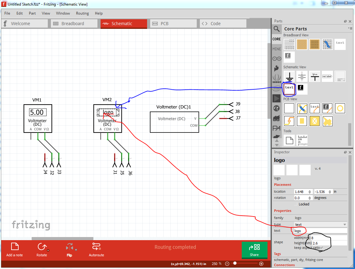
In the schematic view, the part name is not centered on purpose (there is some space below to show the current voltage of the circuit).
I would really appreciate some feedback as I am trying to include them in the fritzing-part repository.
The silk screen is not an “image” in the conventional sense. Silkscreen is a single color, so all svg content (except white I think) is turned into black, and the result used as the svg fill/flood area. What you want is a single color shape (or set of shapes) plus text of what you want the silkscreen to look like. The BB image probably has a whole bunch of overlapping (and filled) shapes, to the result is just a filled rectangle.
Not much wrong. The breadboard svg is missing its layerId which will cause the part to not export as one of the image formats. Easy to correct, at the end of the svg edit, select all in all layers, group it and set the group name to the layerId (breadboard in this case.) The scale isn’t correct, so as this wants to be a core part I corrected it, (instructions here:
I initially added a 7 segment display set to 0.00 then realized you are likely going to use the text function to be able to set a value in a sketch for documenation purposes, and removed my addition as unneeded. The same thing done in schematic below will also work in breadboard. Moved the connectors to be exactly on .1in boundaries to line up with the .1in grid in breadboard (minor position change), in practice unnoticable.
schematic
start from schematic template which has the correct scale connector layout and line widths and colors. Available here:
Added 1 pin to bottom row for the A pin so that schematic matches breadboard, but left it inhibited so it isn’t active in schematic. If you prefer to eliminate the A pin in schematic, just delete it again, either way is acceptable. This image indicates what I meant about adding a voltage value in a sketch (if as seems likely this part is being used to create documentation.) Here from the sketch I added a text field and set the “voltage” to 5.00. As you may know you can change the size with the width and height parameters in Inspector and change the text in the same place as shown here. This also works in breadboard (which is I assume why the display field was left blank.) In general it is desirable for parts in schematic to be as small as possible as room in schematic is limited
Rename the breadboard and schematic svg files to append an _1 i.e. svg.breadboard.multimeter_v_dc_breadboard_1.svg to make a new unique (and more standard) file name. Do the same to the fzp file part.multimeter_v_dc_1.fzp. This will allow this to be a new part that will load along side your current part. Delete icon and pcb svgs, breadboard will be reused as icon and pcb svgs.
fzp file
change the moduleId to multimeter_v_dc_1 (as it must be unique) correct the fritzing version to 0.9.4
change the label to VM (as the first 4 letters of this will become the label VM1, VM2 in this case (although I see it did not in fact truncate your labels, I thought it only did 4 characters …)
change property type to variant (I expect either will work, but variant is more standard)
delete the taxonomy as uneeded (and incorrect in this case!)
insert a trailing _1 (as a version number) before the last breadboard image name:
replace the iconview and pcbview layer names with the above line. That will use breadboard for the icon and as the pcb view (which is effectively no pcb view as the layerIds won’t match)
remove the terminalId from breadboard, as they are not defined in the svg and thus aren’t needed (although while they won’t hurt anything if present, removal is more correct)
remove pcbview entirely as uneeded. Now either run the part file through FritzingCheckPart.py (which is what I did) which will check for a variety of errors and make some xml adjustments. If you don’t want to run FritzingCheckPart, you need to edit each svg file with a text editor and remove the trailing px from the font-size commands, i.e.
because in some circumstances Fritzing will change a font-size ending in px to 0 essentially deleting the text. The CSS standard requires the px in font-size and the svg editors obey CSS. Here is a new version of your part with these changes. If you unzip the fzpz file, you will get the fzp and 2 svgs which you can compare to your original files to see the changes.
Thank you Peter for all your modifications. I will make the other parts and create a pull request to the part repository.
My intention trying to put the image of the bb view in the pcb view was for documenting proposes. Imagine that you need to check something in a pcb with a multimeter, then you could create an image to indicate where to place the probes. In any case, it seems that is not possible with the current code. So, I agree that the best is to remove the pcb image.
Regarding the text on the display of the multimeter, yes there is no text on purpose. You are right, one use case is the one that you describe (I did not think on using the text tools to set the voltage, but it is a realy nice suggestion). My aim is to make a very basic simulator (only dc and no transients) for my students. Still work in progress but getting close. I hope that it could be integrated in the future in the code. A small preview, the link expires in one week.
I’ll poke at this a bit. It may be possible to do something like this (although it may need a code change) similar to adding a ruler (which works in pcb.) It won’t appear in the gerber output but a screen shot of the Fritzing screen would be usable for documentation.
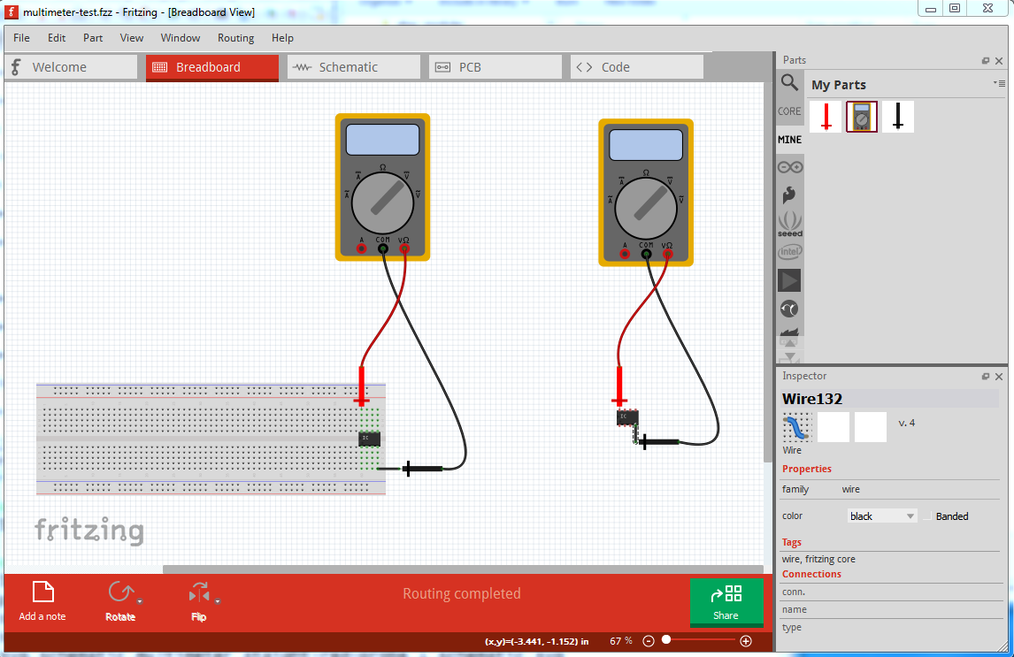
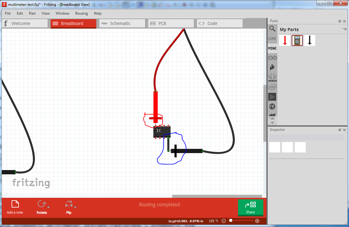
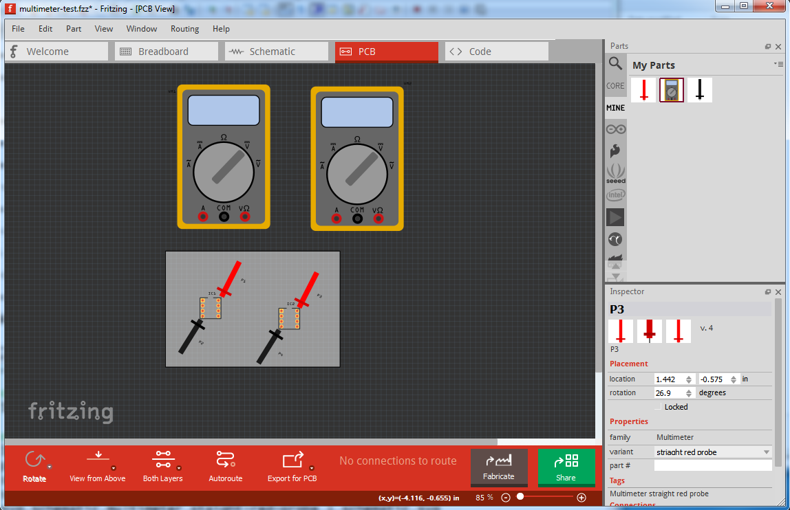
With 2 new parts (for the probes) and a previously undocumented layerId partimage, I have made this work (mostly anyway) in all three views. I suspect partimage is what the rulers use to render in pcb view, but there isn’t any way to attach a wire from the meter to the probes as there is in breadboard or schematic. I expect you could export the pcb image as an svg and use Inkscape to add the necessary wire, but I don’t think Fritzing can do it.
Here as noted the wires from the end of the probe to the meter are not present. As noted you should be able to export this as an svg and use Inkscape to add the necessary wires.
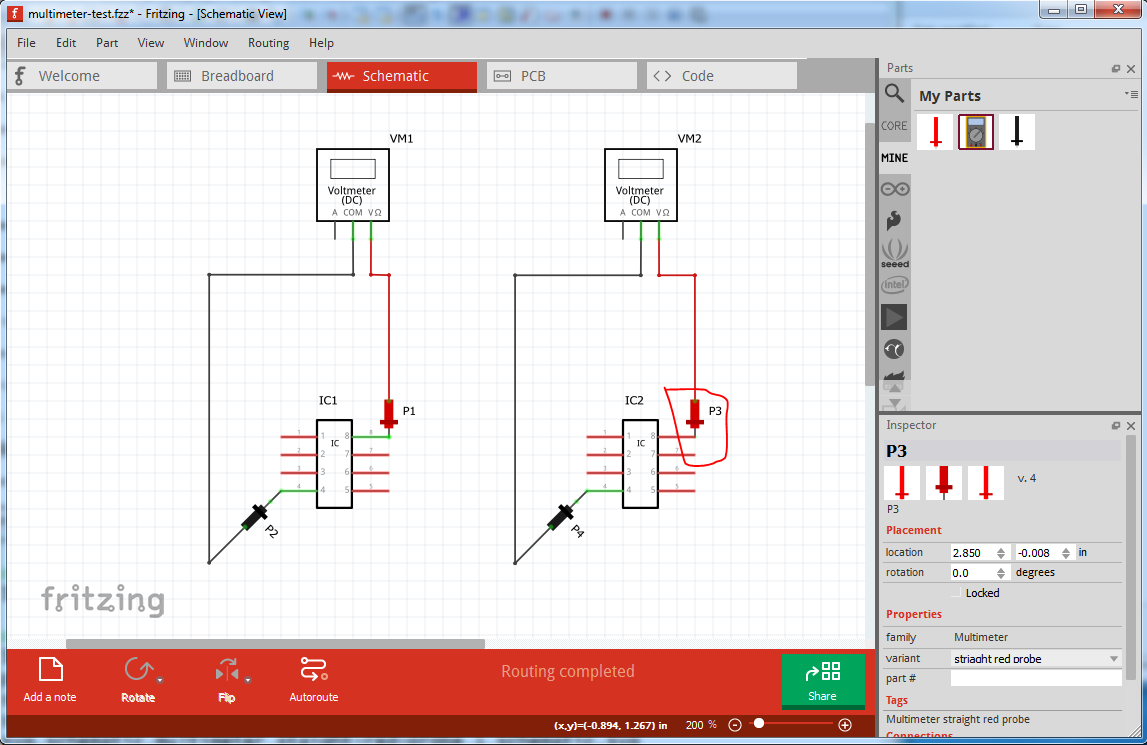
the new pcb layer and connector configuration looks like this:
Regarding the probes, could we change the connector type to wire to fix the issue with male connectors?
I would say that the probes should not have an schematic view. BB and PCB views are physical views where you want to see the real parts. This is not the case in the schematic view and I do not think they are useful. In my opinion, wires to the appropriate nets are enough and provide a cleaner schematic.
I think the probes can be useful for documenting proposes. Of course, it will be to the users to use them or no. For the simulator they are not needed but they will no affect it. Do you mind if I include them in the commit to be included in the core parts?
Regarding the lack of connectors for the multimeter in the PCB view, I wonder if it would be possible to add really small copper pads for the connectors. Thus, the connectors would exist and it would be possible to use jumper wires to connect them to other parts. PCB manufactures will probably ignore anything that is outside the border of the PCB. In case the multimeter is inside the PCB, it will still be safe if the connector is, for example, 0.0001mm in diameter as it cannot be manufactured. The only risk is if the user connects them with normal traces instead of jumper wires.
AFAIK not in a part. Wires are only available in the sketch not in a part.
easy enough to suppress schematic view, either by adding inhibit=“yes” to the fzp file in schematic view or suppressing the schematic view entirely (by replacing it in the layer definitions with breadboard as it needs a renderer.)
Not at all, feel free to add them, thats what they are for.
The problem is the new layer doesn’t have any conception of connectors. So while you could add pads, they won’t move with the probes (as they do in breadboard) because there isn’t an association between the pad and the image.
Based on the Part file format documentation, the type wire and pad exists. I just tried it and a connector of type=“wire” connects to male and female connectors. However, the connection is kept when you separate the two parts (similar as when you have a wire). No ratsnets are created in other views but the connectors of both parts highlight when you highlight te connectors at the same potential (when the parts are no longer connected). So, let´s discard this.
I am thinking that another work around would be to create two connectors at the same place. One female and another male. Thus, the probes will connect to both female and male connectors. Does it seem a feasible solution? I do not want to submit parts that could create new issues (for example if they just connect to female connectors).
But would not be possible to add another layer to the pcb view. For example, copper0 layer and add the pads in that layer? Thus, we could have the partimage and copper0. I guess that the layers will move together.
It may be, you could try it and see. I think there are currently some bugs in this area though because some things that should connect do not.
You can do that, but it is not connected to the partimage layer, so if you move the partimage layer you would manually need to move the pad on the copper layers to match. As well the connector in the copper layer will appear on the board.
I tried with the male and female connectors for the probes. It works, but I found a bug in Fritzing and report it. Only works if a part with male connectors (e.g a resistor) is moved to a part with female connectors (the probe).
Regarding removing the probes from the schematic view, I could not make it work by adding inhibit=“yes” to the fzp file. Is this documented anywhere? I could not find it in the part wiki documentation. So, finally, I just pointed to the breadboard layer and it works.
In any case, I made a pull request. You can review it here:
Mmm. Now, I realized that if I do not add the schematic view of the probes, the netlist is broken (there is no connection between the connectors of the probe). I just activate the schematic view again.
Any ideas of how to do not have an image but leave the connectors? If not, I guess that the easier is just leave the probes in the schematic view. Or maybe modify them to be a bit more schematic like. For example, Kicad has something like this: