Having completed all the files for the part in (and earlier):
http://forum.fritzing.org/t/part-creation-howto-part-3-fzp-file/7695
On to testing the part.
First run it through FritzingCheckPart.py, the part checking script. This checks the syntax of the part for errors and fixes some things that Inkscape does for CSS compliance that Fritzing does not support. Those are: remove the px from the end of font-size elements. Replace CSS style commands with equivalent inline XML (bendable legs do not support style commands), and insure that a stroke-width value (which may be inherited) appears in the copper1/copper0 groups (because gerber processing doesn’t do inheritance and will break without a stroke-width.) FritzingCheckPart.py is available from:
So to start download the broken fzp file created in the last part of this series:
part.S4A_EDU_1-errors.fzp (40.4 KB)
and copy it to part.S4A_EDU_1.fzp
then download the 3 svg files created in parts 1 and 2 of this series:
svg.breadboard.S4A_EDU_1_breadboard.svg.fzp (180.5 KB)
svg.pcb.S4A_EDU_1_pcb.svg.fzp (15.4 KB)
svg.schematic.S4A_EDU_1_schematic.svg.fzp (106.7 KB)
again you need to remove the trailing .fzp to recover the .svg file (because the forum has problems uploading svg files.) Then install FritzingCheckPart.py from github above if you have not and run FritzingCheckPart.py like this (this is under cygwin on Windows.) Note I used a newer version of the script that hasn’t been released yet because it has better formatted output messages so this output may not exactly match what you get until the new version is released but the error numbers should be the same, just the text is poorly formatted:
$ FritzingCheckPartw.py part.S4A_EDU_1.fzp
**** Starting to process file Startup, no file yet
**** Starting to process file part.S4A_EDU_1.fzp
Error 6: ParseFile error parsing the input xml file part.S4A_EDU_1.fzp
part.S4A_EDU_1.fzp:12:53:FATAL:PARSER:ERR_TAG_NAME_MISMATCH: Opening and ending tag mismatch: url line 12 and unparseable
The xml error in the fzp file at line 12 as the error message above stated here somewhat cryptically:
part.S4A_EDU_1.fzp:12:52:FATAL:
                   ^^ ^^
		  |  |
		  |  | char on line
		     |
		     | line number
so edit the .fzp file with a text editor (here I am using vi under cygwin but any text editor should work) and correct line 12:
$vi part.S4A_EDU_1.fzp
where:
<url>https://www.gotronic.fr/pj2-34440-1407.pdf</>
should be
<url>https://www.gotronic.fr/pj2-34440-1407.pdf</url>
So use your text editor to correct that and try again:
$ FritzingCheckPartw.py part.S4A_EDU_1.fzp
**** Starting to process file Startup, no file yet
**** Starting to process file part.S4A_EDU_1.fzp
**** Starting to process file svg.schematic.S4A_EDU_1_schematic.svg.bak
**** Starting to process file svg.pcb.S4A_EDU_1_pcb.svg.bak
File
‘part.S4A_EDU_1.fzp.bak’
This is a through hole part as both copper0 and copper1 views are present.
If you wanted a smd part remove the copper0 definition from line 43
Modified 4: File
‘svg.schematic.S4A_EDU_1_schematic.svg.bak’
At line 31
ReferenceFile
‘S4A_EDU_78c08539140e87873a7d0ebd198bd086_1_schematic.svg’
doesn’t match input file
‘S4A_EDU_1_schematic.svg’
Corrected
Modified 1: File
‘svg.schematic.S4A_EDU_1_schematic.svg.bak’
At line 50
Removed px from font-size leaving 60
Modified 1: File
‘svg.schematic.S4A_EDU_1_schematic.svg.bak’
At line 56
Removed px from font-size leaving 49
… (many more identical lines removed to save space!)
Modified 1: File
‘svg.schematic.S4A_EDU_1_schematic.svg.bak’
At line 212
… (many more identical lines removed to save space!)
Modified 1: File
‘svg.schematic.S4A_EDU_1_schematic.svg.bak’
At line 3330
Removed px from font-size leaving 49
Modified 4: File
‘svg.pcb.S4A_EDU_1_pcb.svg.bak’
At line 16
ReferenceFile
‘S4A_EDU_78c08539140e87873a7d0ebd198bd086_1_pcb.svg’
doesn’t match input file
‘S4A_EDU_1_pcb.svg’
Corrected
Warning 34: File
‘svg.pcb.S4A_EDU_1_pcb.svg.bak’
At line 752
translates are undesirable.
Error 15: Can not rename
‘svg.breadboard.S4Ar_EDU_1_breadboard.svg’
to
‘svg.breadboard.S4Ar_EDU_1_breadboard.svg.bak’
‘svg.breadboard.S4Ar_EDU_1_breadboard.svg’
No such file or directory (2)
Error 20: File
‘svg.breadboard.S4Ar_EDU_1_breadboard.svg’
During processing svgs from fzp, svg file doesn’t exist
Error 18: File
‘part.S4A_EDU_1.fzp.bak’
Connector connector21terminal is in the fzp file but not the svg file. (typo?)
svg svg.schematic.S4A_EDU_1_schematic.svg.bak
Error 18: File
‘part.S4A_EDU_1.fzp.bak’
Connector connector53pin is in the fzp file but not the svg file. (typo?)
svg svg.schematic.S4A_EDU_1_schematic.svg.bak
Error 18: File
‘part.S4A_EDU_1.fzp.bak’
Connector connector54pin is in the fzp file but not the svg file. (typo?)
svg svg.schematic.S4A_EDU_1_schematic.svg.bak
Error 18: File
‘part.S4A_EDU_1.fzp.bak’
Connector connector65pin is in the fzp file but not the svg file. (typo?)
svg svg.schematic.S4A_EDU_1_schematic.svg.bak
$
Which produces this huge bunch of output. The Modified lines like these can usaully be ignored (that is why they are output first in the listing, so they are there but easy to ignore). They document the changes the script has made to the various files in case something goes wrong.
This one records that the orginal reference file ‘S4A_EDU_78c08539140e87873a7d0ebd198bd086_1_schematic.svg’ was replaced with the svg file name ‘S4A_EDU_1_schematic.svg’ as it should be. As far as I know Fritzing doesn’t care about reference file names, but this is the correct value.
Modified 4: File
‘svg.schematic.S4A_EDU_1_schematic.svg.bak’
At line 31
ReferenceFile
‘S4A_EDU_78c08539140e87873a7d0ebd198bd086_1_schematic.svg’
doesn’t match input file
‘S4A_EDU_1_schematic.svg’
Corrected
Next we have a large bunch (all the text in the svgs) where the trailing px was removed from the font size. If the px is left on the font-size and the svg is processed by the New parts editor, the font size will be set to 0 which means the fonts will be tiny instead of their proper size. This is likely a Fritzing bug, but it hasn’t been fixed yet (and may not be fixable if its a QT issue.)
Next we have the warning messages. These are as the name implies Warnings, something is unusual, but not known
to break Fritzing. It is issued to alert the human to look at the issue and see if it is in fact an error that needs to be fixed
Warning 34: File
‘svg.pcb.S4A_EDU_1_pcb.svg.bak’
At line 752
translates are undesirable.
It is complaining about translates in polygons in breadboard, which I don’t know of a way to remove yet (it may not be possible except ar render time). It is intended to warn you that there are translates in a svg which it is desireable but not always possible to remove (some in pcb are marked as Error because they will break Fritzing.) Here we can ignore this (with the original script currently on github you won’t see this message)
Now come the important ones the Errors that need something done about(When I finish the new version of this script it will be added to the tool change for parts submission and in order to get a part included in core parts, all the Error conditions will need to be removed.):
Error 15: Can not rename
‘svg.breadboard.S4Ar_EDU_78c08539140e87873a7d0ebd198bd086_2_breadboard.svg’
to
‘svg.breadboard.S4Ar_EDU_78c08539140e87873a7d0ebd198bd086_2_breadboard.svg.bak’
‘svg.breadboard.S4Ar_EDU_78c08539140e87873a7d0ebd198bd086_2_breadboard.svg’
No such file or directory (2)
the breadboardfile image is misnamed (an extra r) in the fzp file, so correct that.
<breadboardView>
  <layers image="breadboard/S4Ar_EDU_1_breadboard.svg">
which should be:
<breadboardView>
  <layers image="breadboard/S4A_EDU_1_breadboard.svg">
Note there is some truth to the opinion that this is why you should use the New parts editor to edit parts, because it does not make mistakes like this. If that works for you, then using New Parts editor is fine. For me it doesn’t work in enough cases that I prefer to do this and deal with the errors I create.
Next there are several pins misnamed in the schematic svg file which also need correcting (in this case the
error isn’t in the fzp file because the connectors in the fzp file were created correctlly by a script leaving only the svg, in a normal part it could be either, so you need to check both).
Error 18: File
‘part.S4A_EDU_1.fzp.bak’
Connector connector21terminal is in the fzp file but not the svg file. (typo?)
svg svg.schematic.S4A_EDU_1_schematic.svg.bak
This is telling you that connector21terminal is defined in the fzp file (and we see as noted it is spelled correctly because it was generated by a script rather than me typing), but a corresponding id was not found in the scheamatic svg svg svg.schematic.S4A_EDU_1_schematic.svg.bak. The .bak on the end is because that is the original svg.schematic.S4A_EDU_1_schematic.svg which was saved as a backup before the script processed the file. The .bak file is used here because the line numbers in svg.schematic.S4A_EDU_1_schematic.svg may be different if certain modifications were made by the script to the svg file. I usually ignore the .bak file and edit the svg.schematic.S4A_EDU_1_schematic.svg file remembering the line number may be out a line or 2 either way. In this case the fzp file doesn’t know what line number the terminal it can’t find should be in the svg, and thus doesn’t provide a line number so we need to search for the listed pin (which is probably misspelled). This is where it is useful to have the terminals in order on the bottom of the xml editor window. That makes it easy to find connector21terminal which in the svg file is connectort21erminal which needs to change to connector21terminal to match the fzp file. Similar things for the other pins and terminals with the error and correction listed below:
connector53tpin
to
connector53pin
connector54pi
to
connector54pin
and then
lconnector65pin
to
connector65pin
Now run
$ FritzingCheckPart.py part.S4A_EDU_1.fzp
again, which will now complains about breadboard because it didn’t process it the fist time due to the file name error:
… (px removed warnings snipped)
Warning 34: File
‘svg.breadboard.S4A_EDU_1_breadboard.svg.bak’
At line 52
translates are undesirable.
Warning 34: File
‘svg.pcb.S4A_EDU_1_pcb.svg.bak’
At line 752
translates are undesirable.
Error 18: File
‘part.S4A_EDU_1.fzp.bak’
Connector connector15pin is in the fzp file but not the svg file. (typo?)
svg svg.breadboard.S4A_EDU_1_breadboard.svg.bak
$
If the pins in breadboard were not in order (which may not be because of how the connectors are constructed, where moving the connector to the bottom of the xml window modifies the appearance of the connector) it is neccessary to search for the connector in Inkscape. To do so load the svg in Inkscape and then click in the xml editor window to select something, (anything will do), then press cntrl-f, Inkscape is being uncooperative and closes the search window when I switch to snip tool. In Inkscape a blank rectangle appears in the xml editor window that you type the search term into in this image:
bb-xml-element-selected.PNG
in the box that comes up type connector15 which finds nothing, so switch to r15 which finds
cnnector15pin
which needs to be
connector15pin
In this case because the pins are in order you can more easily just scroll down to connector15 though. Now run FritzingCheckPart.py again:
$ FritzingCheckPart.py part.S4A_EDU_1.fzp
**** Starting to process file Startup, no file yet
**** Starting to process file part.S4A_EDU_1.fzp
**** Starting to process file svg.breadboard.S4A_EDU_1_breadboard.svg.bak
**** Starting to process file svg.schematic.S4A_EDU_1_schematic.svg.bak
**** Starting to process file svg.pcb.S4A_EDU_1_pcb.svg.bak
File
‘part.S4A_EDU_1.fzp.bak’
This is a through hole part as both copper0 and copper1 views are present.
If you wanted a smd part remove the copper0 definition from line 43
Warning 34: File
‘svg.breadboard.S4A_EDU_1_breadboard.svg.bak’
At line 66
translates are undesirable.
$
and this time it runs clean. The warnings about px are missing because they were removed on the first run through of the script and are thus no longer a problem. If you had to edit the svg in Inkscape they may have returned as Inkscape re adds the style and px for CSS.
If you did not choose to reuse the breadboard svg as the icon image file, copy the breadboard svg in to the icon svg (checkpart ignores icon svgs, so it is desirable to have the corrected breadboard svg in there).
use 7zip (or any other zip program) to create the fzpz file from
part.S4A_EDU_1.fzp
svg.breadboard.S4A_EDU_1_breadboard.svg
svg.pcb.S4A_EDU_1_pcb.svg
svg.schematic.S4A_EDU_1_schematic.svg
Note 7zip will allow you to rename the default .zip file to .fzpz, if your zip program won’t create it as a zip file and then rename the .zip to .fzpz.
to a file called S4A-EDU-improved.fzpz to create the new part.
Start Fritzing and
open->S4A-EDU-improved.fzpz
which immediately shows a problem:
in schematic view the part is showing as “part1” because there is not a label element in the fzp file so go correct that first. Open the fzp file in a text editor and make this change to add a label field:
  <title>Tarjeta S4A EDU</title>
  <url>https://www.gotronic.fr/pj2-34440-1407.pdf</url>
to
  <title>Tarjeta S4A EDU</title>
  <label>Mod</label>
  <url>https://www.gotronic.fr/pj2-34440-1407.pdf</url>
Now you need to rezip the fzpz file to make the above change, and now when you load the part it should be labeled Mod1 not part1.
At this point (before routing the test connections to avoid having to redo that!) export and check the gerber files. To do that, with the part the only thing in pcb view, (if needed, it is not in this case, in Inspector increase the size of the pcb from the default 56.4mm to fit the pcb and drag the pcb background til the entire pcb is present like this:
Then click on File->Export->For production->extended gerber (RS-274X) and select a directory to store the gerber files and click Select folder to write the gerber output to that directory. When that is done, edit the Untitled Sketch_drill.txt file in the directory where the gerbers were written and check the hole sizes (in this case they are all 0.038in for .1 square headers). If they are not as expected (i.e. one or more are some odd value due to an error), correct that first before proceding to route the test sketch (because you will just need to waste time redoing the test sketch after you fix the drill sizes later.) In this case they are correct because I copied in the pcb of headers made correctly by the parts factory. This is from a sketch that someone posted to the forums (because it has a wrong hole size):
Untitled Sketch_drill.txt
; NON-PLATED HOLES START AT T1
; THROUGH (PLATED) HOLES START AT T100
M48
INCH
T1C0.086614
T100C0.015748
T101C0.038000
T102C0.035000
T103C0.036076
T104C0.040000
…
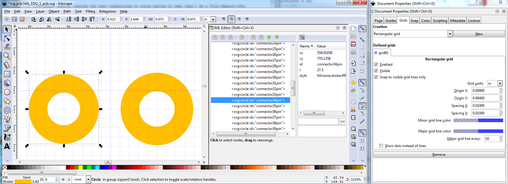
In the above the line “T103C0.036076” is wrong (this is the DFRobot DFPlayer Mini part in core parts at present.) The hole for a .1in header pin should be 0.038in (like the line two above it) not 0.036076in. At this point you should go back to the pcb svg and correct the pads involved to adjust the hole size to 0.038in (or whatever the data sheet specifies for the hole.) In Inkscape the hole diameter is set to hole diameter = pad diameter - 2 * stroke-width. At the 10.41667 scale used here and the standard 20 thou stroke width, we produce a 0.038in hole by 20 (stroke-width) * 2 = 40 + 38 (0.038 inches in thou) = a pad diameter of 78 thou. A complication in Inkscape is that the start position of the hole is the edge of the pad, but pitch is to the center of the hole. The lazy way out of this is to select a pad, then in the tool bar set the height and width of the pad to 0.078in and record the radius value from xml editor. Now use Edit->undo to undo the height and width change, then in xml editor set the radius to the value you found by changing the height / width above. An example using a pad from this part’s pcb svg to illustrate this process. First I will change the radius of an existing pad so the pitch is correct (at .1 in) but the hole size is not (it is 0.035in rather than 0.038 as it should be) (note: I adjusted the grid offset in Document properties here so the pads are centered on the grid to demonstrate the change in offset):
Now I set the smaller pad’s diameter from 0.075in to 0.078in via the tool bar (highlighted in blue) and we see the pitch of the pad changes slightly to the right in x and up in y (highlighted in red):
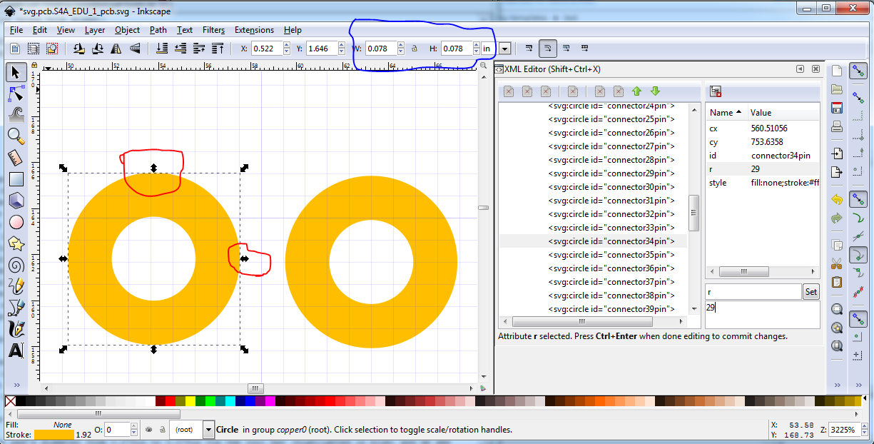
So take note of the new radius in xml editor (29 instead of 27.5) and then Edit->undo change attribute twice to reset the diameter to 0.075in. Now instead of changing the diameter via the tool bar, in xml editor change the radius from 27.5 to 29.
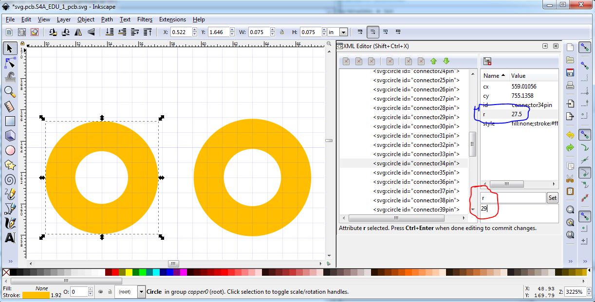
That changes the size of the pad to 0.078in but leaves the center of the pad where it is, which is what we need to preserve the proper pitch:
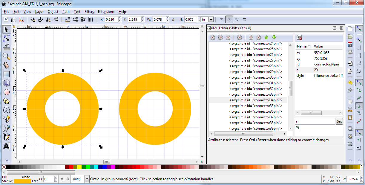
As we see the pad is now the same size as the one next to it, and in the correct x/y position. Job done.
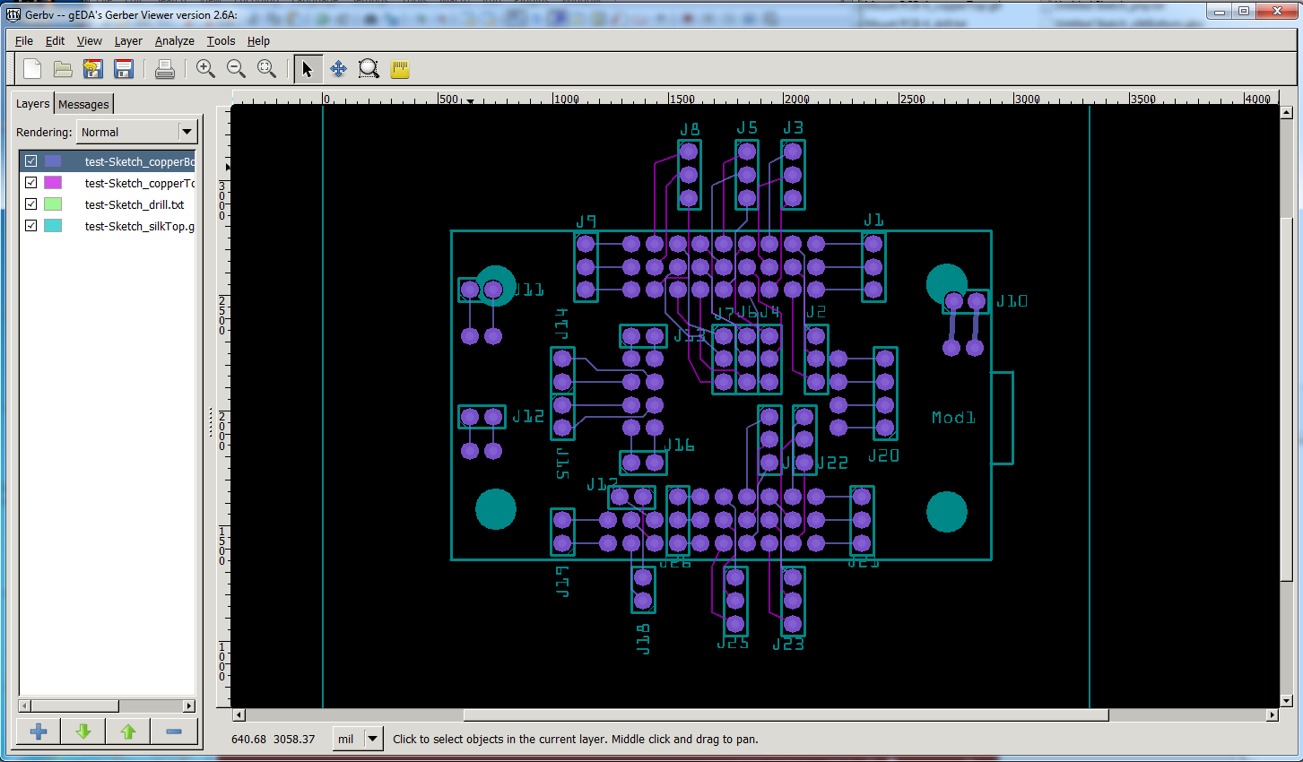
Now using a gerber viewer (I use gerbv from the Geda project, but there are lots of them) load the copper0 (if there is one, SMD parts only have copper1), copper1, drill, silkscreen top, and silkscreen bottom layers. Check that everything that appears on those layers in Fritzing’s pcb view is present. There are bugs where sometimes an element is displayed correctly in Fritzing PCB view, but is incorrect (outline paths in silkscreen are a common one) in the gerber output. Since the gerber output (not Fritzing pcb view) is what makes the board, the board will be wrong. If there are problems here, correct them before going on with the testing so you don’t have to redo the later testing (laziness ruling yet again!) Next That isn’t always the case if you started from another part though. The line “T100C0.038000” indicates that hole type T100C (plated through hole) will be drilled to the desired 0.038in.
; NON-PLATED HOLES START AT T1
; THROUGH (PLATED) HOLES START AT T100
M48
INCH
T100C0.038000
…
Now before you route the test sketch, check the bus configuration, if there is one in your part (there is in this one and there is an error here.) To do that, with the part loaded in to Fritzing, pick one of the three views (I usually use schematic because the pin labels there make it easy to check the members of the bus are correct), and click on a pin that is a member of the bus. All the other pins that are supposed to be in the bus should light up yellow. If one or more do not, or a pin not in the bus lights up, there is a bus error and you need to fix that before proceeding. In this case (since there is a bus error in this part) lets try it. With the Tarjeta-S4A-EDU-improved.fzpz loaded in to Fritzing, click on the isp-5 pin RESET. It should not be bused as RESET isn’t an external pin, however it is bused to D11 due to a typo in the fzp bus definitions (connector66 instead of cconnector64 as it should be), so edit the fzp file and correct that:
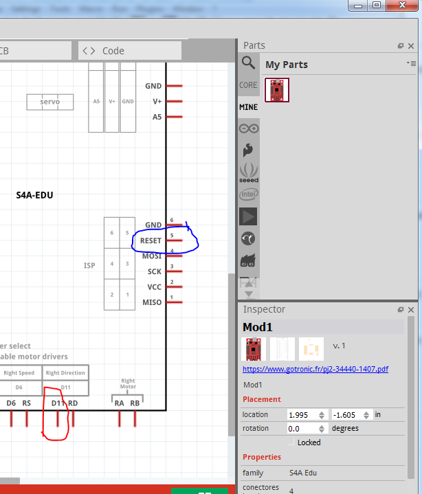
(the yellow highlight only exista as long as the pin is hovered over in Fritzing, hovering over the Reset pin outlined in blue here should incorrectly light D11 yellow.) To correct this edit the fzp file in a text editor and correct the bus definition for the D11 bus:
<bus id="D11">
  <nodeMember connectorId="connector42"/>
  <nodeMember connectorId="connector66"/>
</bus>
should be
<bus id="D11">
  <nodeMember connectorId="connector42"/>
  <nodeMember connectorId="connector64"/>
</bus>
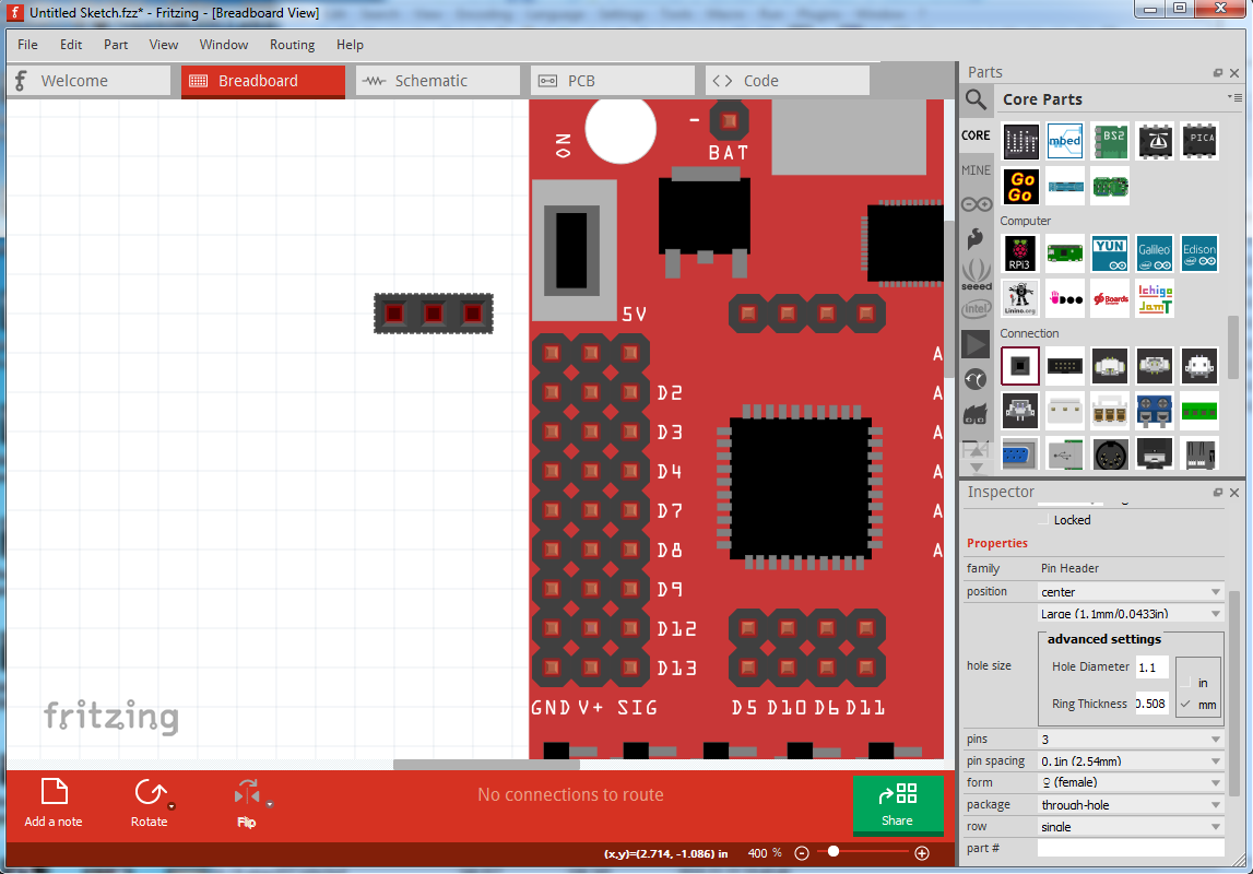
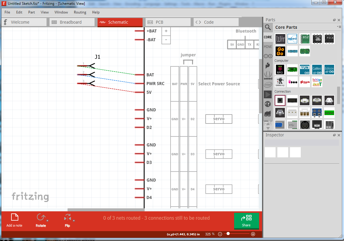
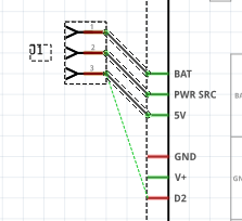
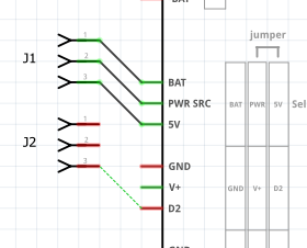
so correct that and rebuild the fzpz file with 7zip load it and make sure clicking on D11 lights isp-4 MOSI rather than isp-5 RESET as now. At this point we have verified the pcb to gerber and bus definitions are correct so now we can route the sketch to verify all the connections. To do that I use connectors of the appropriate length to work in scehamtic (someiimes as in this case connectors in breadboard are different in schematic). Note due to a current Fritzing bug (which hopefully will be fixed in an upcoming release), you are best off to drag a part in to schematic first. If you drag it in to breadboard or pcb, its orientation in scheamtic will be random (i.e. correct sometimes but rotated others.) Dragging it in to schematic first normally places it correctly oriented. So lets start testing the part (which typically takes almost as much time as making it!) Because the servo pins are odd (i.e. different in schematic than in breadboard) I will start there by creating a 3 pin connector for the top row of the three 9 pin headers like this:
Laziness tip: the connector will likely be misaligned in schematic, aligning it correctly in schematic before duplicating the next eight for the other conneectors in breadboard will save re aligning later ones in schematic.
now switch to schematic to align the connector (which is indeed incorrectly aligned and needs to be flipped horizontal):
So right click on the connector and click flip horizontal to change it to the correct alignment and move it in to the correct position like this:
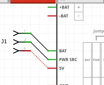
Of note here is the end of the connector is two grid marks up and two grid marks left of the end of the connector. The purpose of this is to check both the alignment and the position of the connector terminalId. If the terminalId is missing (which the check script should catch) the connection will be to the center of the pin like this:
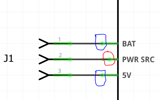
with the connector offset from the pin, the error becomes obvious:
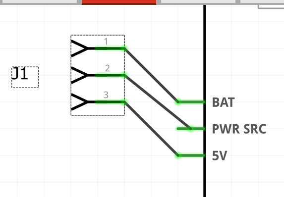
which is why to use the offset pin layout. Now switch to pcb view to route the connector there (this avoids confusion later when all the connectors align on top of each other.) First use inspector to increase the height of the background pcb from the default 56.4mm to 100mm to give more space for connectors (if they are outside the grep pcb area, they will be truncated in the gerber output!):
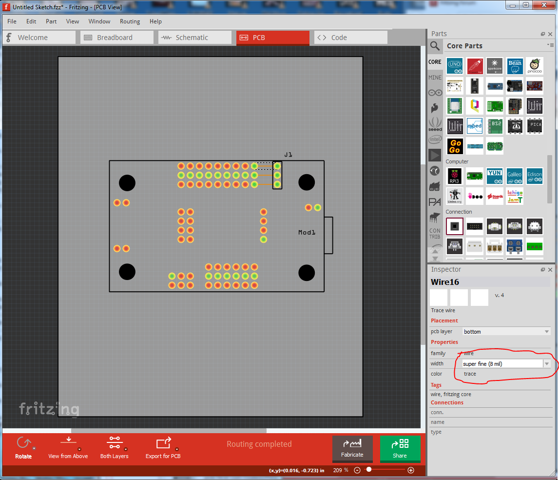
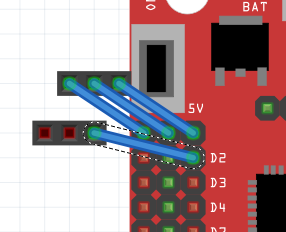
of note here is I moved the connector in pcb in to position, routed it (all on the bottom level) and set the trace widths to super fine 8mil (8 thousandth of an inch) in Inspector (outlined in red), as sometimes the traces will need to go between pins. Note this isn’t a practical routing, the idea is to verify that the pins connect to the correct place so, I don’t care about whether the placement makes physical sense or not. Now switch back to breadboard and duplicate the first connector to use for the second one. Now switch back to breadboard view and select the first connector, right click it and duplicate it.
which appears correctly aligned in schematic (although overlayed on the first connector):
click and drag it in to position:
and laziness wins, you don’t have to flip in horizontally and move the pin label. There is however an issue:
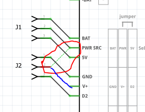
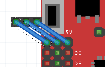
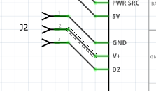
here because the middle connector is bused, and the connection on the pin above it is closer to the second pin, the rats nest line connects to the incorrect connector. That isn’t a problem, you just need to click on +V pin on the part and drag that to the pin on the connector (shown poorly by a blue line in the image) to make the correct connection like this:
Now because I am lazy and don’t want to redo all the work I have jumped to the isp connector where we come on an error, breadboard is fine:
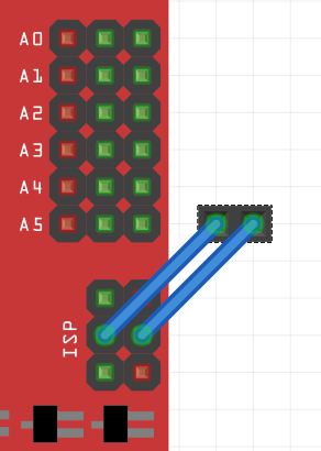
but schematic has a terminalId offset by .1in (which the script won’t catch, as the terminalId is present, just in the wrong position) which causes this:
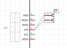
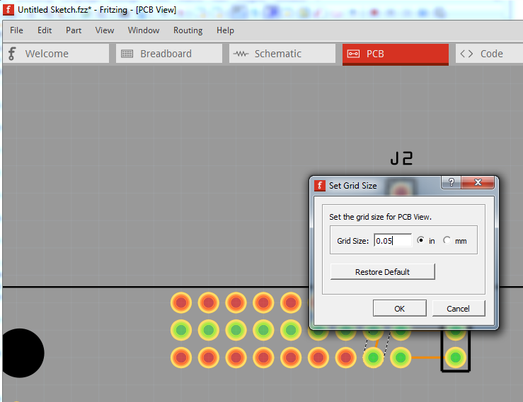
here the connector64terminal and connector65terminal y coord are the same rather than .1in different. Thus both the lines from the connector connect on pin3 rather than one on pin 3 and one on pin4 as should happen. To correct this you need to correct the position of connector64terminal in the schemaitc svg. In this case the visual check finds an error that is difficult for automated tools to find. Now back to pcb to route the second connector. To do that we need to set the grid size finer than the default .1 in so in Fritzing in pcb view click on view->Set grid size and set the grid size to .05in like this:
that allows you to route the second connector like this (without shorting any of the other pads):
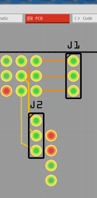
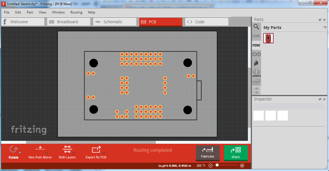
Now route all the rest of the part to end up with this:
test-Sketch.fzz (73.9 KB)
Once pcb is all routed run DRC (Routing->Design Rules Check) to make sure your part has sufficient clearance. For some high density SMD parts you may need to adjust the DRC rules to make it pass, but it is preferable to be able to pass the defailt rules if possible. As the last step, export the pcb view as gerbers (File->Export->For production->Extended gerber (RS274X) and check the result in a gerber viewer to make sure pcb view is being correctly reflected in the gerber output (there are some bugs in the gerber code, so this isn;t always true.) The gerber output from gerbv for this particular sketch looks like this:
When all that passes, your part is ready to publish.