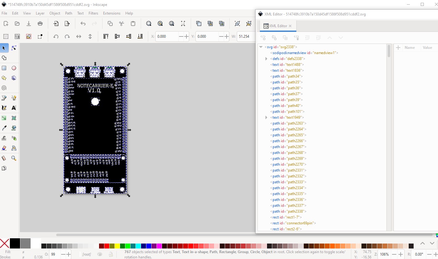
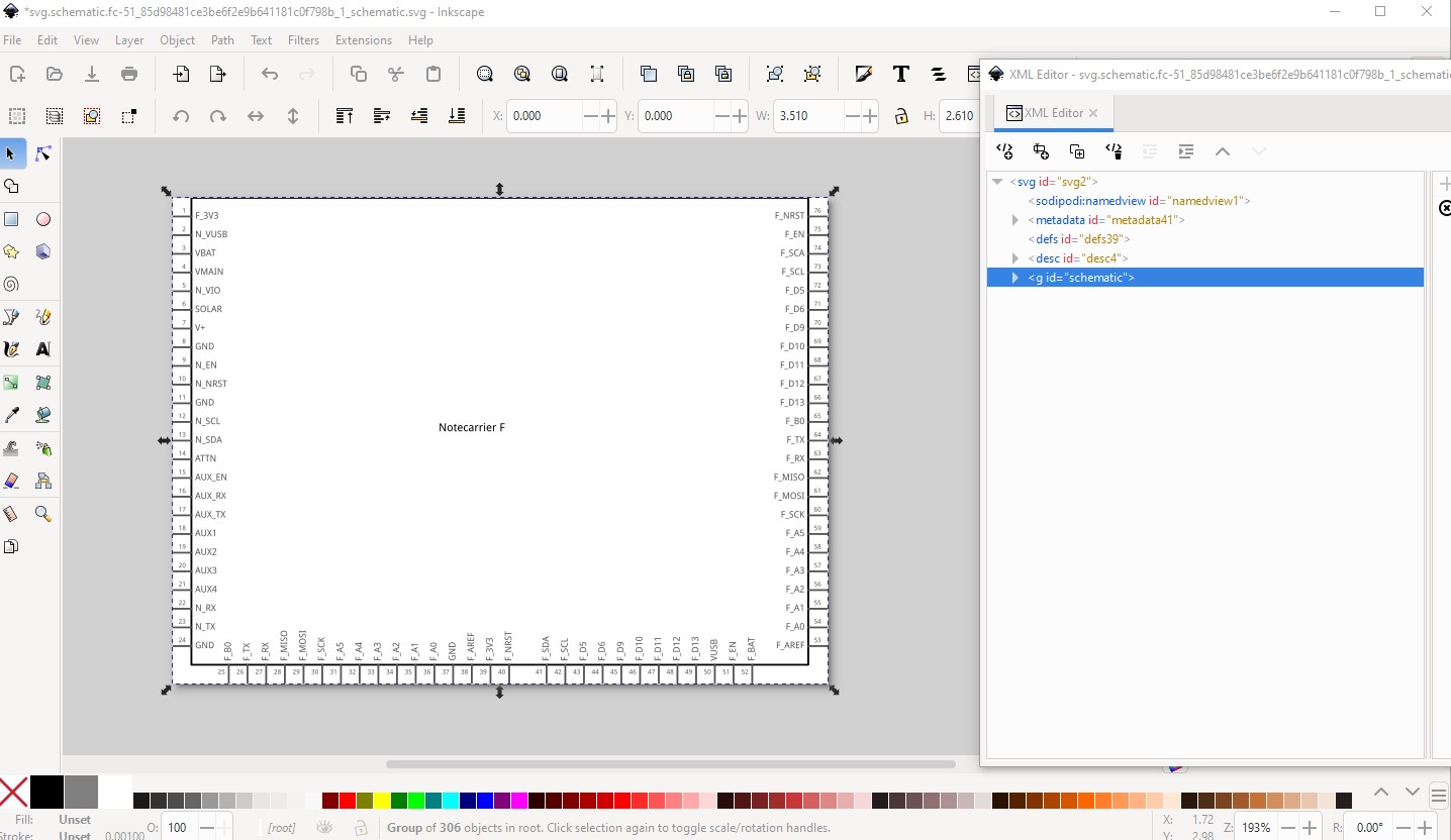
I have been trying to create a fritzing version of Notecarrier F, and so far, this is what I have. When I transfer it to fritzing, the pins are not showing.

I did try to search for it online but couldn’t find it. They’ve posted the kiCad files here. I have been using them as references for mine. I’m not sure how to create the PCB and schematic view. any help is welcomed.
At present there isn’t one it appears (a google search for “fritzijng part Notecarrier F” doesn’t turn one up.) There is this post in their forums that says they are thinking about one from 2022 so you may wish to supply them with one if you complete it.
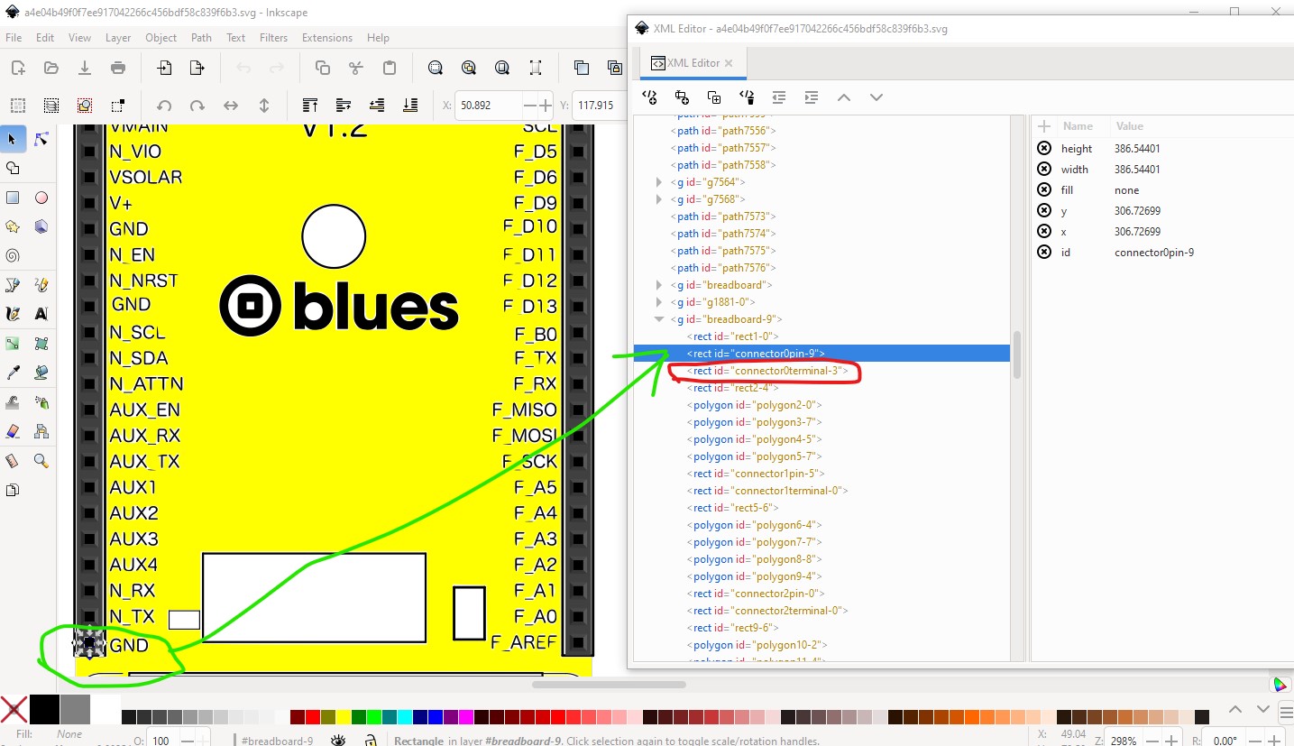
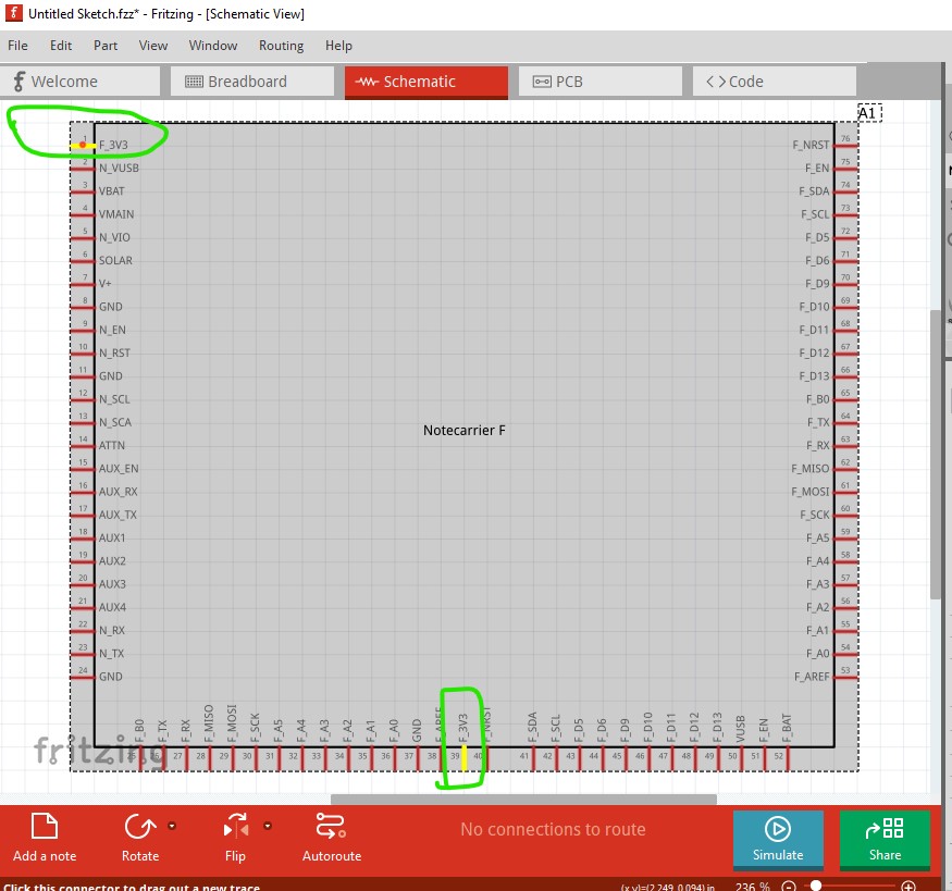
That said your svg has connectors although the grouping and numbering aren’t correct:
You need a group that encloses the entire svg labeled “breadboard” to set the layerId (without it your part won’t export as an image.) I would remove the terminalId (circled in red) as it isn’t needed in breadboard (you need to remove it from the .fzp file if it is in there as well though!) The following tutorial may help you do this:
The likely problem is that the connector numbers don’t match what is defined in the .fzp file and they need to for the connectors to be recognized. This is a snippet of an fzp file with the connector definitions:
      <connector id="connector0" type="male" name="Pin 1">
        <description></description>
        <views>
          <breadboardView>
            <p svgId="connector0pin" layer="breadboard"/>
          </breadboardView>
          <schematicView>
            <p svgId="connector0pin" layer="schematic" terminalId="connector0terminal"/>
          </schematicView>
the labels in your svg need to match the ones in the. .fzp file and likely don’t (connector0pin-9 in the svg file likely isn’t defined in the fzp file and thus isn’t considered a connector.) FritzingCheckPart.py will check your finished part and complain about a variety of errors (in general warnings won’t break a part but errors usually will.) The pins should start at connector0pin on the top left and go up in sequence. Using Randy’s Inkscape schematic extension I would put the left connectors on the left (starts at connector0) then the bottom 2 connectors on the bottom and the right connector on the right with nothing on the top (they need to be in that order for the extension to work correctly.) I have scripts (although not all are published) to renumber pins in the svg if the connectors are the last thing in the svg, again that is covered in the tutorial I think. Schematic is easiest to generate from Randy’s Inkscape Fritzing schematic extension which will produce a properly scaled and configured schematic svg from table input values. It takes a little getting used to, but is far easier than doing it manually. I would likely skip pcb view (how to do that is covered in the tutorial) as it isn’t likely to be useful I don’t think this appears to mostly want connecting wires rather than be intended to mount on a pcb. You have made a good start, but there is a fair way yet to go. Feel free to ask for help if you run in to problems (uploading either the .fzpz file or the svgs preferably so there is something to work from!) which you look to already know how to do.
Peter
I have tried to incorporate some of your feedback, and this is as far as I can go.

OK, so I have fixed up some problems in your breadboard svg, and created (and documented how) a schematic and fzp file to create a working part for this board, which (to cut to the chase) is here:
notecarrier_f.fzpz (56.8 KB)
in case you don’t care to read the rest of this (which is rather long) which describes how I created this part. Starting from the latest svg above I did an edit->select all then grouped the entire svg.
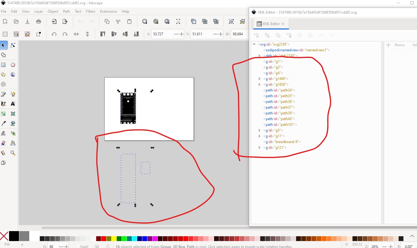
note there are a bunch of unused paths well below the svg, they will get deleted later.
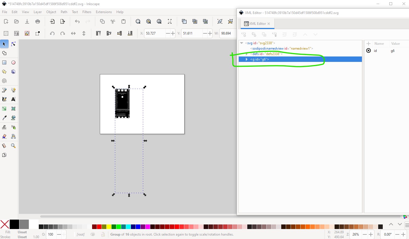
Now I selected that group and ungrouped it multiple times which removes all the groups (and incidentally most transforms) from the svg like this
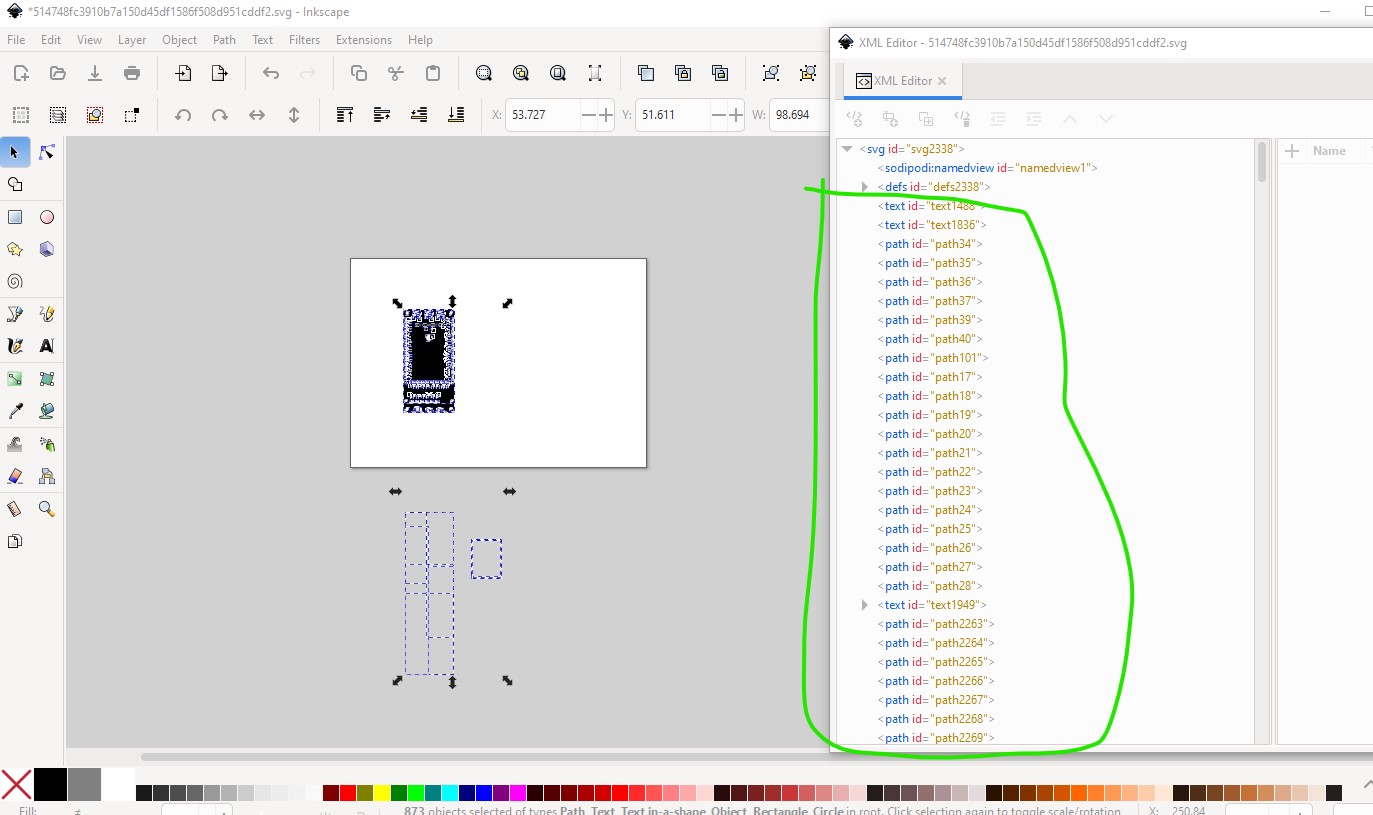
next I deleted all the paths at the bottom which are unused (circled in red here)
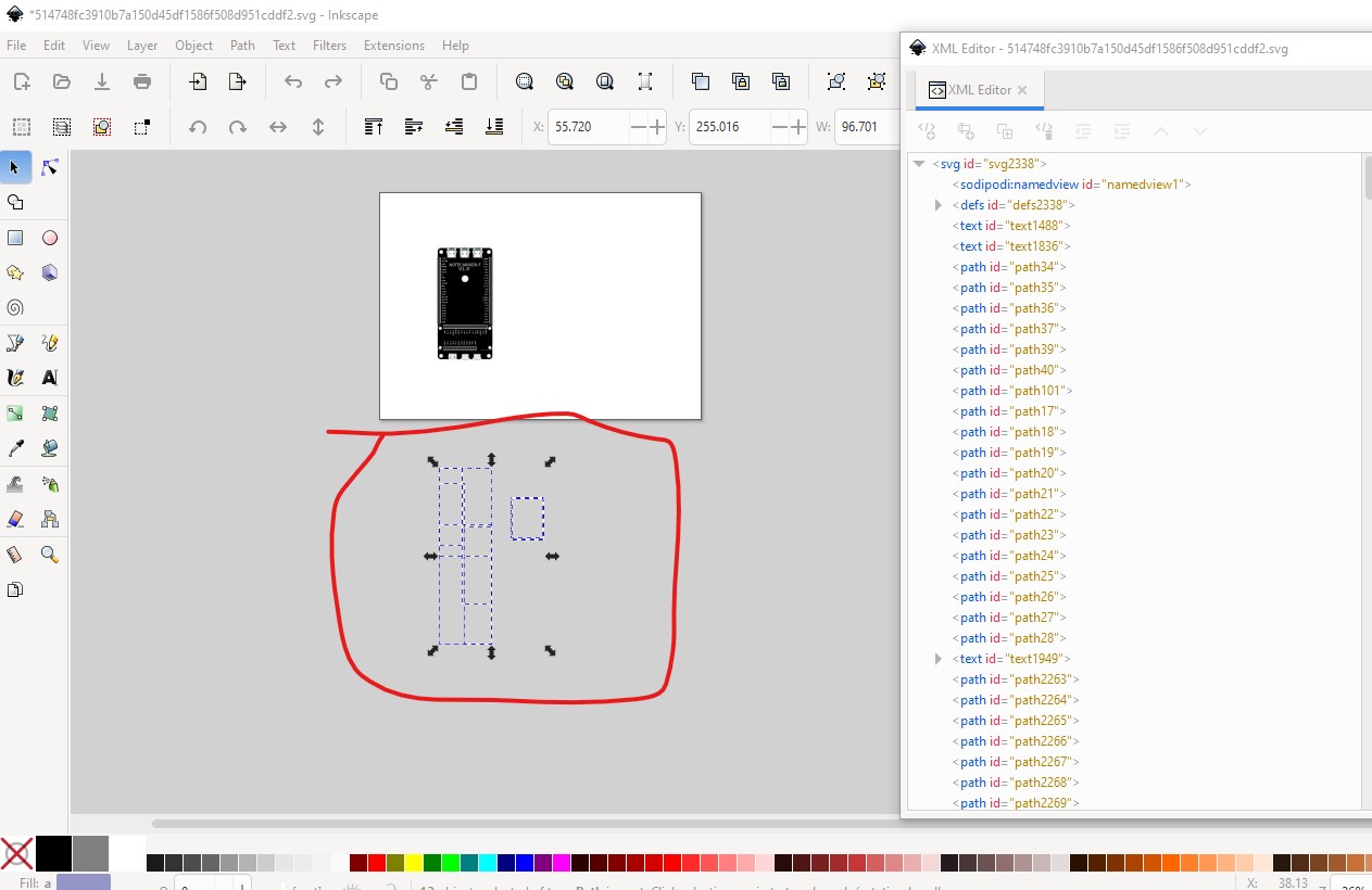
which leaves us with this:
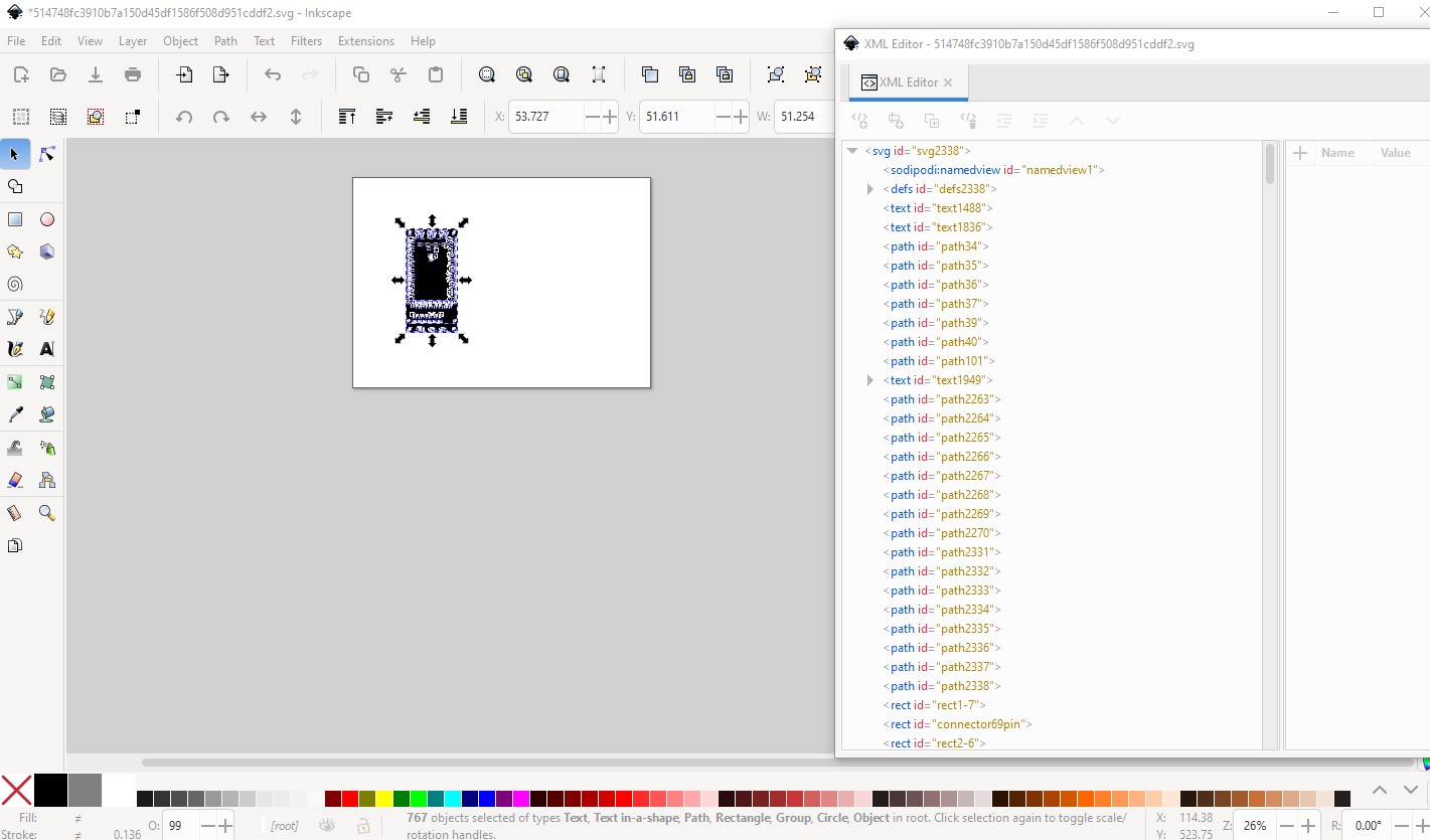
then (this is all in Inkscape!) I did a resize page to selection to resize the viewbox
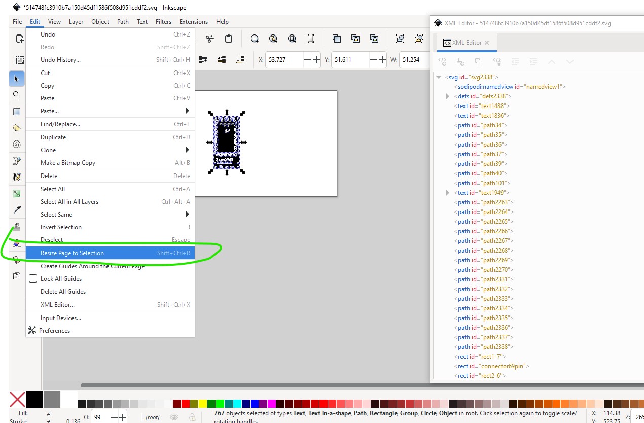
which results in this
then I rescaled the svg to the scale specified in the graphics standards (where one drawing unit = 1/1000in) by setting the format to inches and setting the scale to 0.001 like this
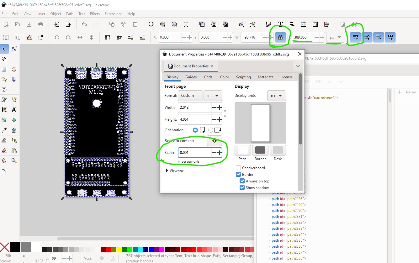
note the changes to the tool bar settings circled in green at the top (the procedure for doing this is documented in the tutorial.)
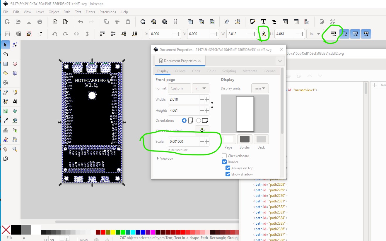
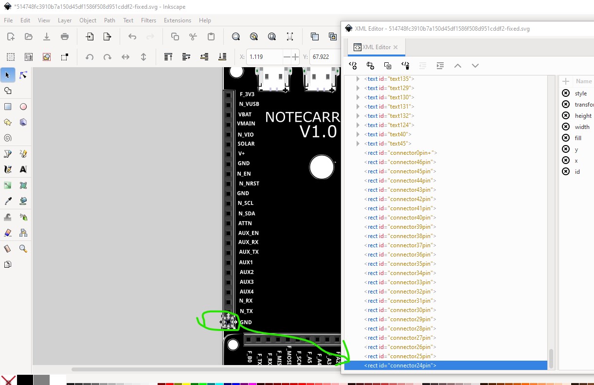
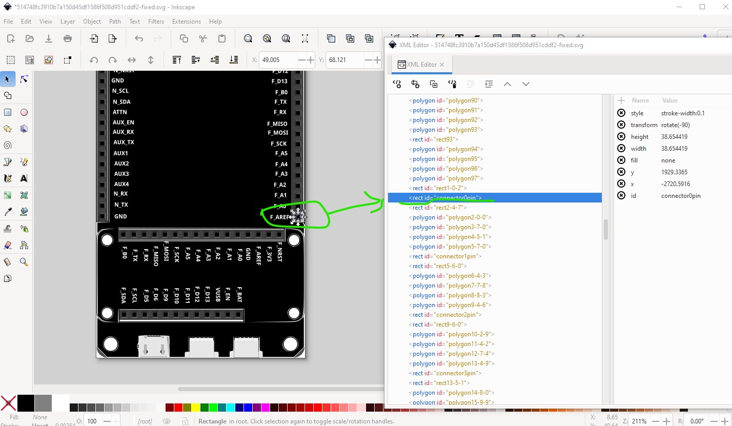
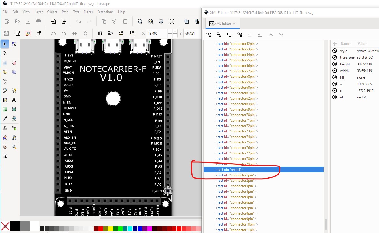
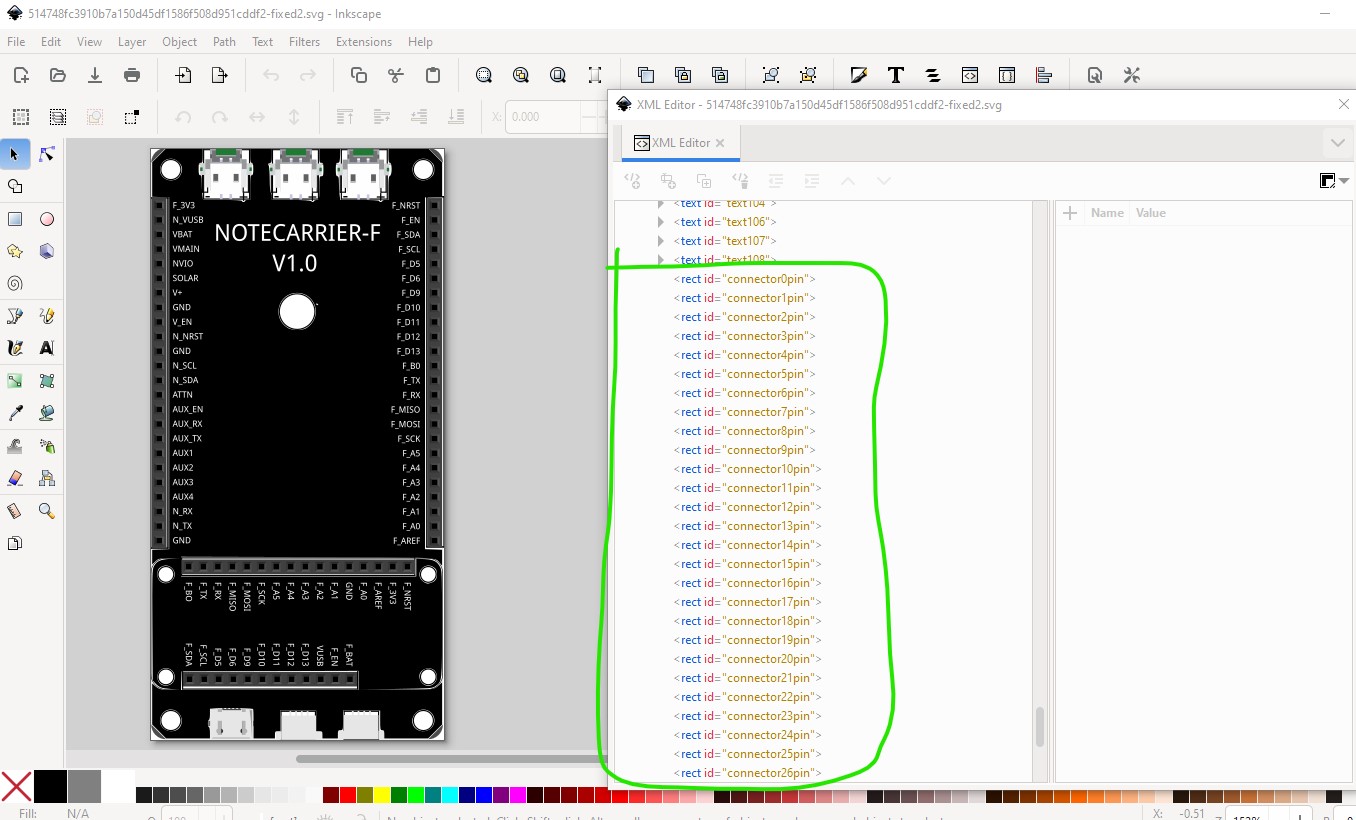
Then I reset the lock horizontal to vertical and scale stroke settings back to normal to proceed. Now we are going to select the various connectors starting with connector0pin (which wants to be the top left connector.) To do that I selected an element in the correct connector like this and then stepped back up in the xml editor window to identify the connector (circled in green) and moved it to the bottom of the svg like this
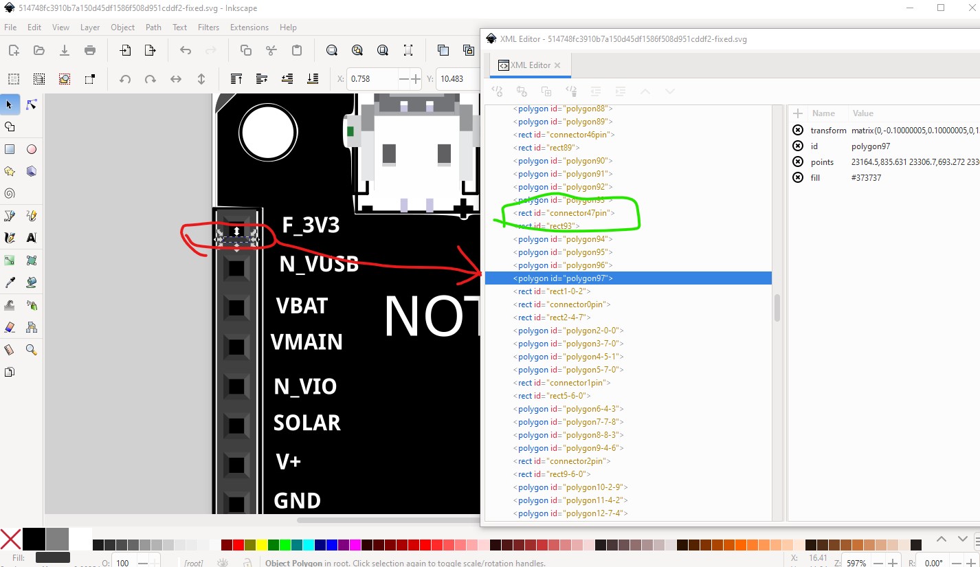
checking that it is the correct connector by clicking on it in xml editor which selects it in the svg
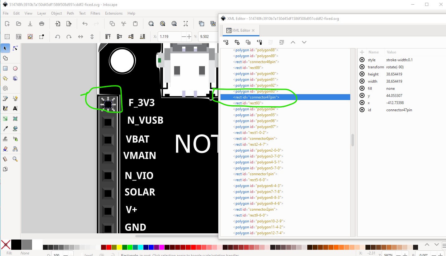
then click on the toolbar icon (circled in red here) to move the element to the bottom of the svg
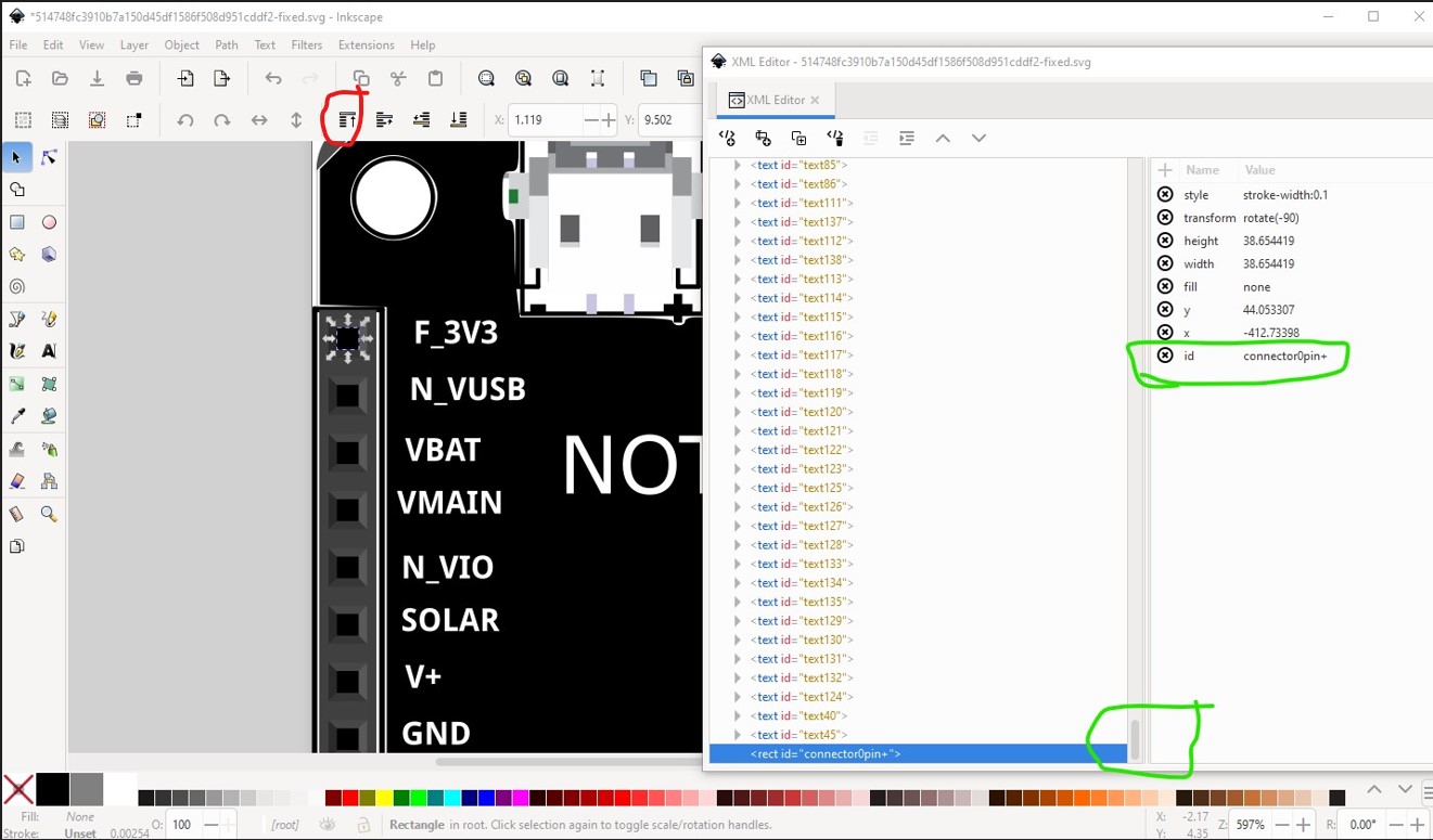
and change the id to “connector0pin+” to mark the new connector0 pin (the + is to avoid an existing connector0pin from being renamed and thus lost in the svg.) Then move to the next pin down
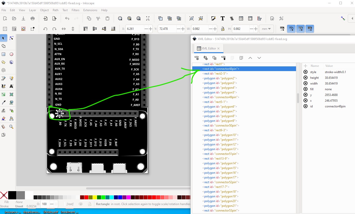
and repeat the procedure and continue on to the end of the connector
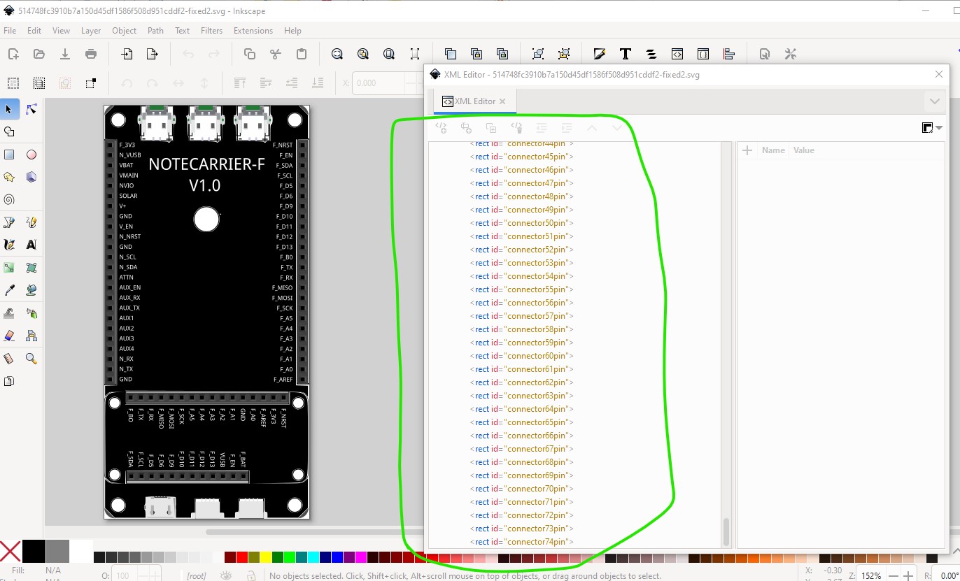
now we switch to the first pin of the connector on the bottom (which in schematic is going to be on the bottom of the schematic) which needs to be in this order for the schematic extension to work correctly
til the end of that connector
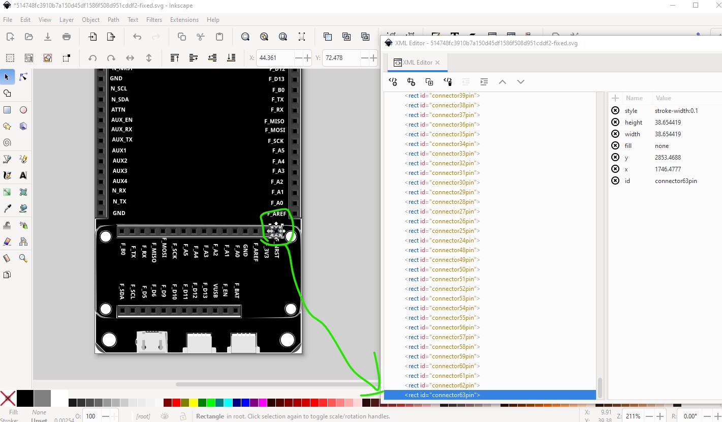
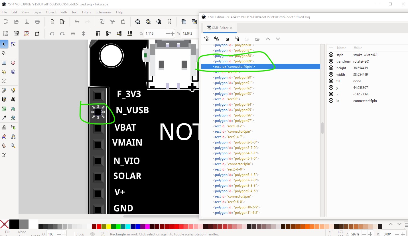
and then on to the first pin of the lowest connector
followed by the connector on the right
til the top of that connector
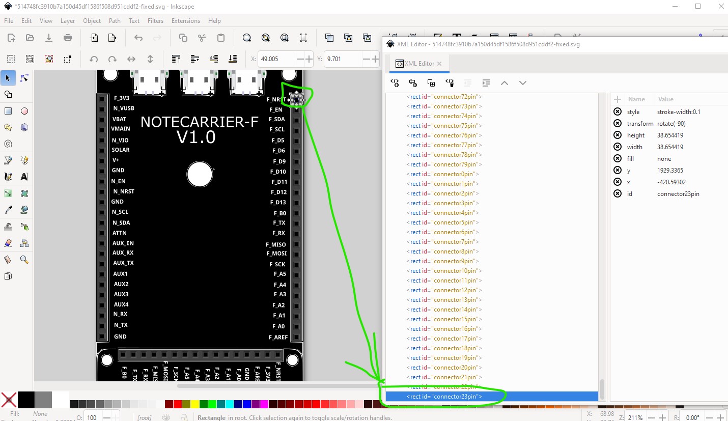
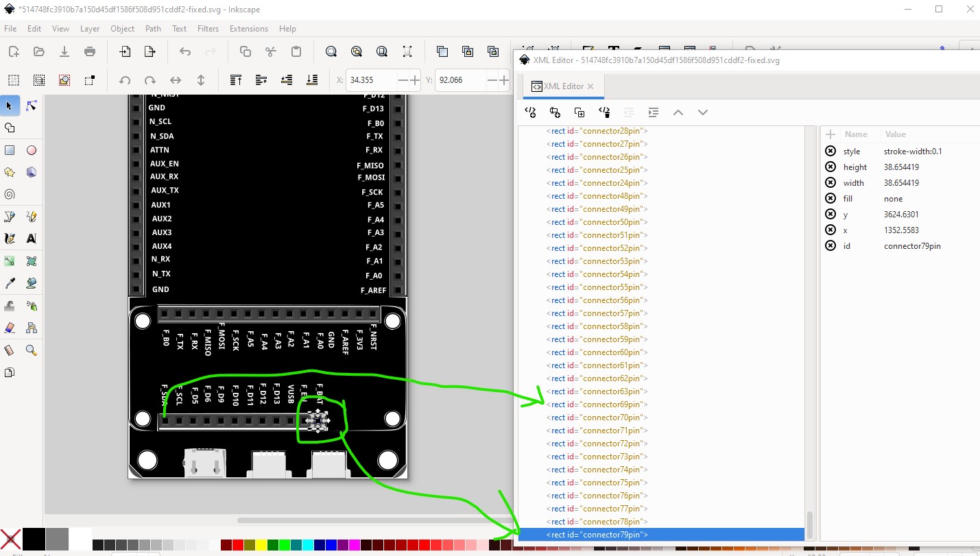
which completes the selection of connectors. Now go back to connector0pin+ and change its id to connector0pin
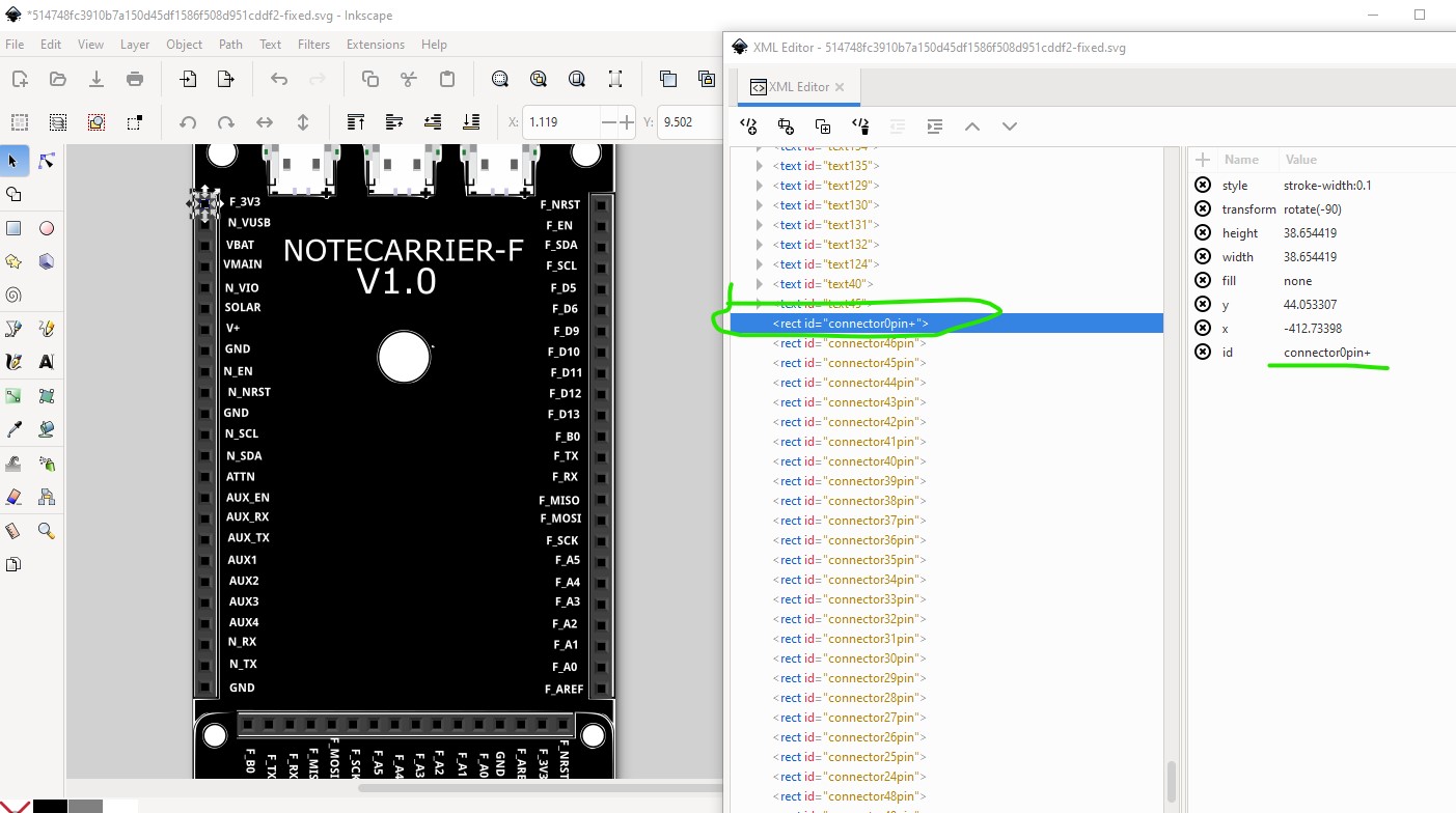
like this
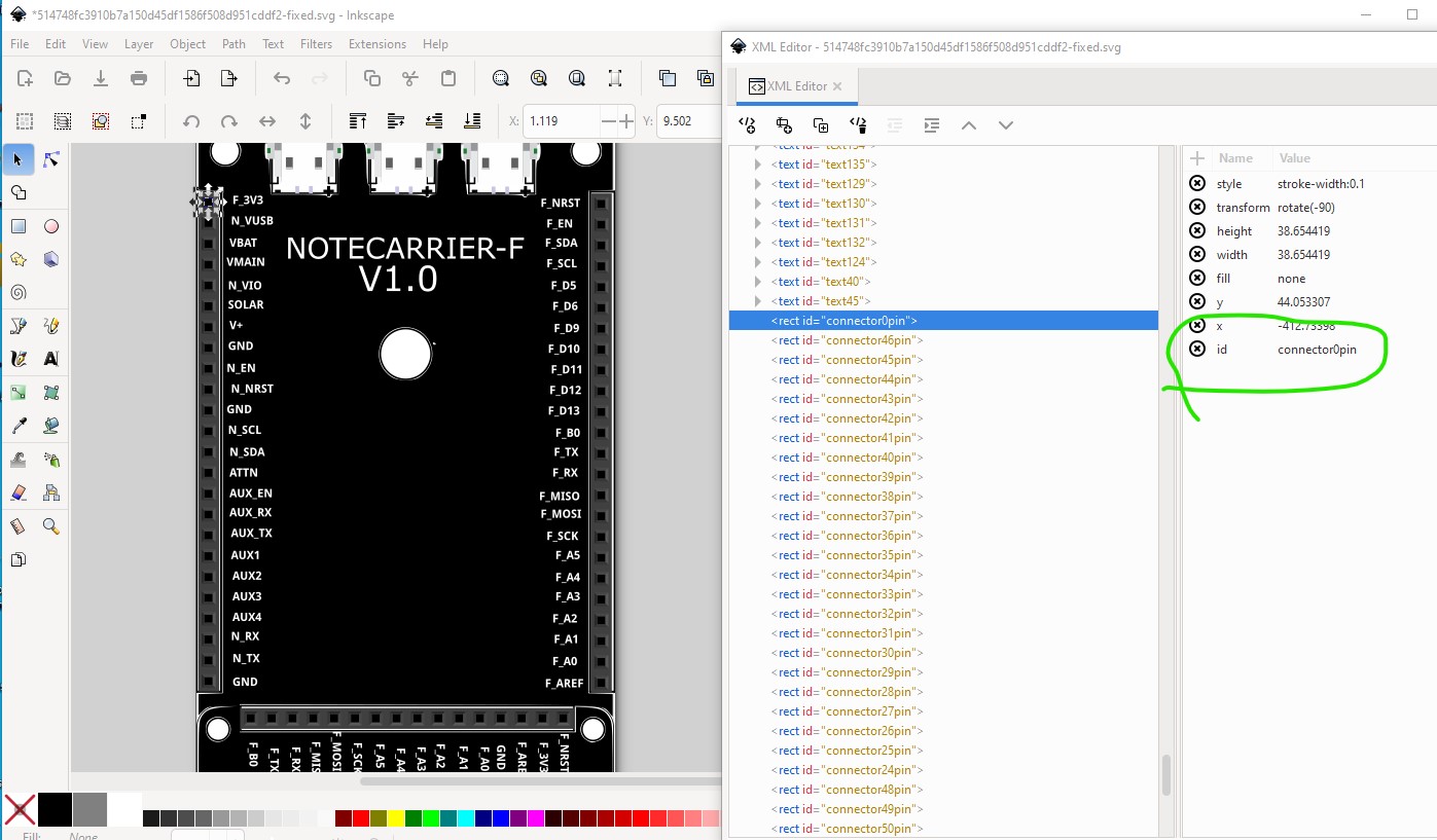
note the old connector0pin has been replaced by a new label by Inkscape which is why not to do this before now.
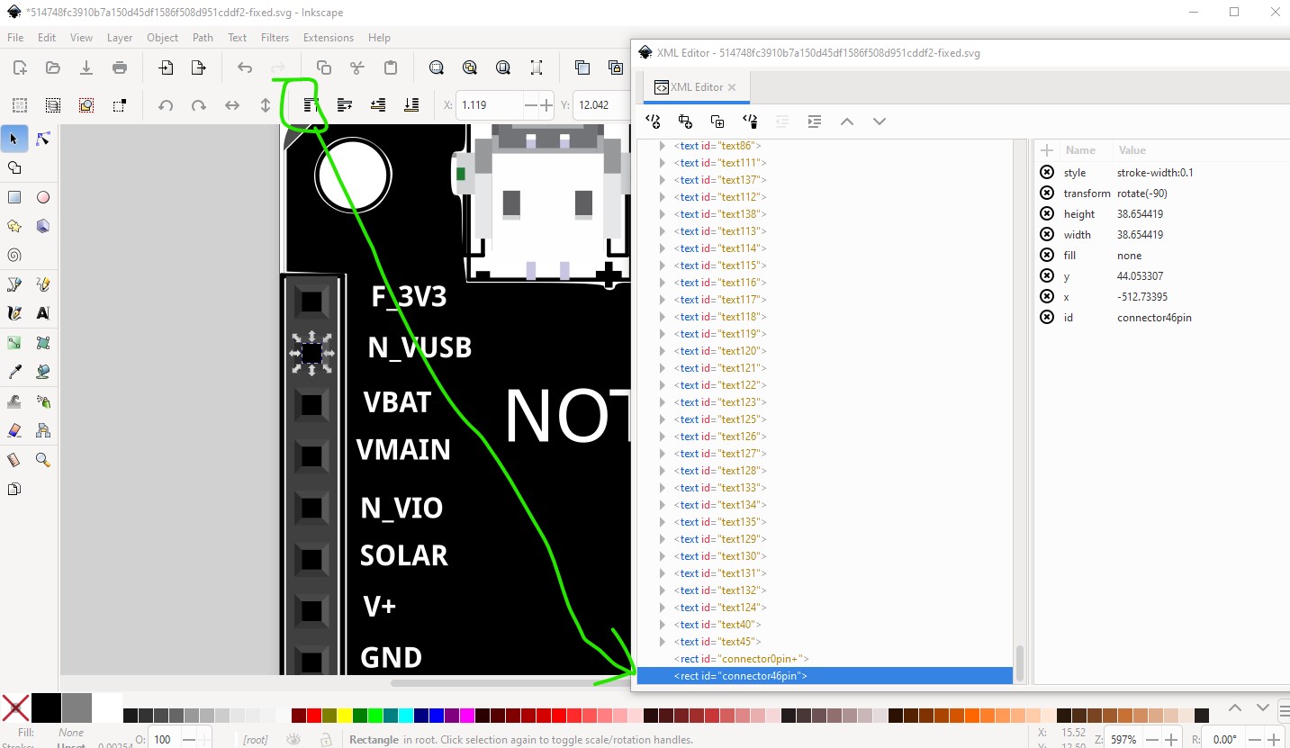
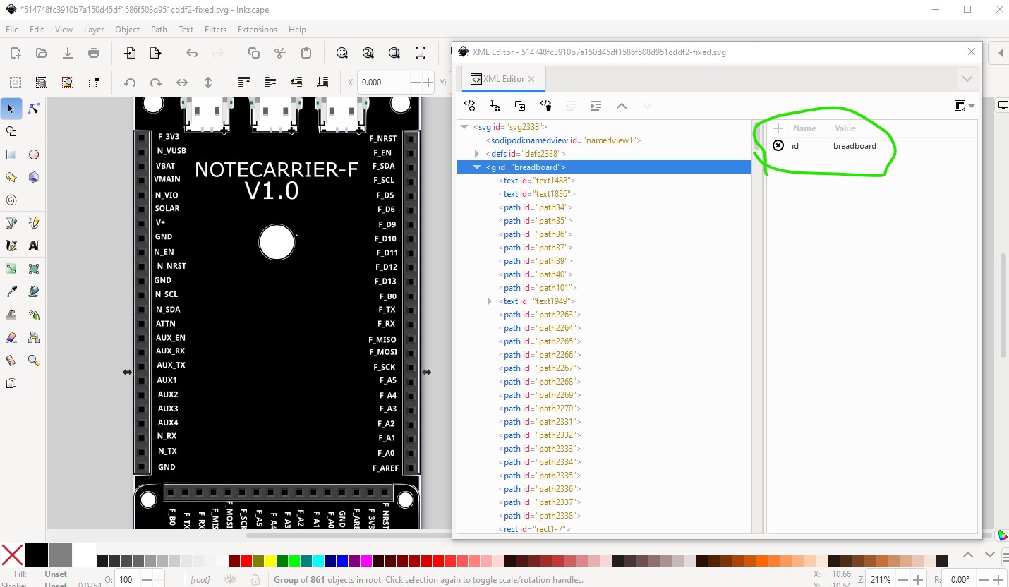
then do an edit->select all and object->group and name the resulting group (which encloses the entire svg) as breadboard to set the layerId like this
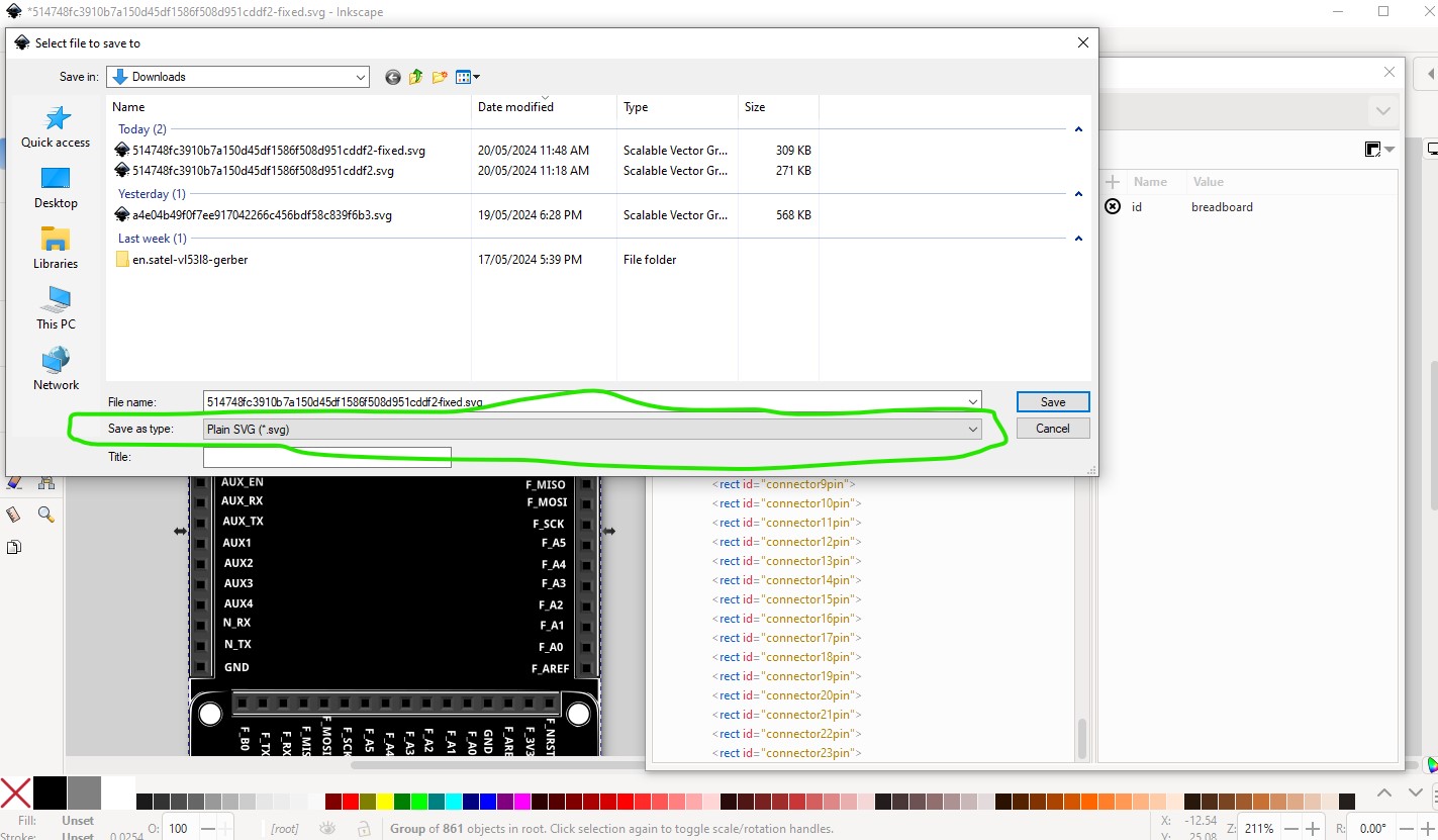
now select File->save as and change the Save as type from Inkscape SVG to plain SVG (Fritzing prefers the plain svg setting rather than the Inkscape version.)
to save the modified svg (this should be done for all Fritzing svg files!) Now I ran setbb.py against the svg file just created. That scans the svg looking for connector0pin and when it finds it renumbers the pins starting at 0 and increasing by 1 which results in an svg that looks like this
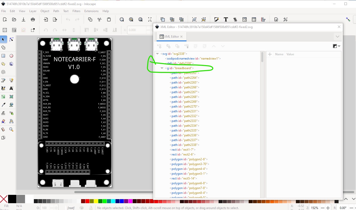
with the pins properly numbered. This is slightly wrong as I discovered later that one of the pins in the lowest connector had its connector relabeled (probably due to a conflict) which I needed to correct later. That means there is one less connector here than there should be.
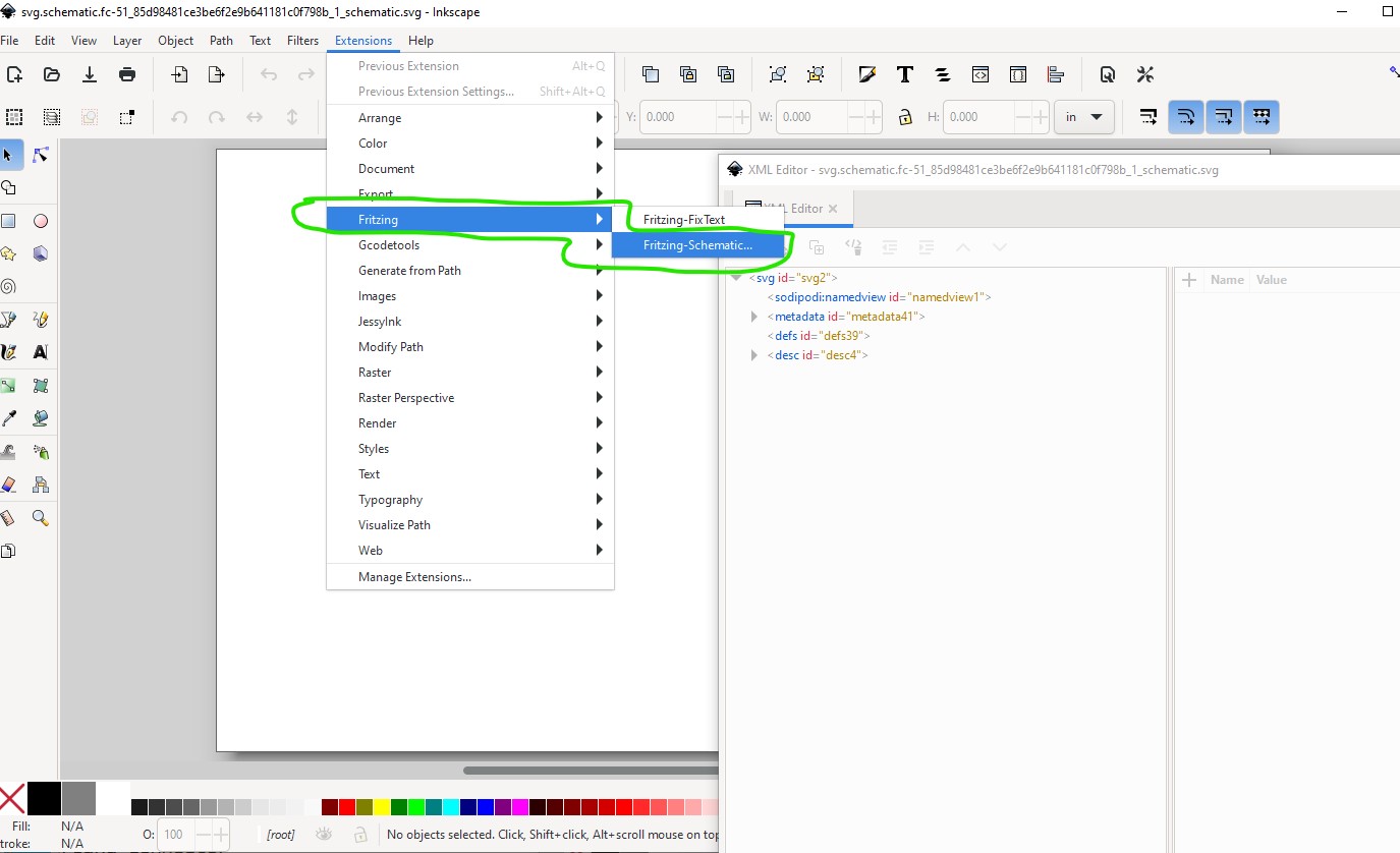
the last pin should be connector75 not 74. So now breadboard is complete on to schematic. As noted I have Randy’s Fritzing schematic extension loaded in to Inkscape so start it.
then set the parameters (note the width should be 3.2in not 3.0 but that is correctable later.)
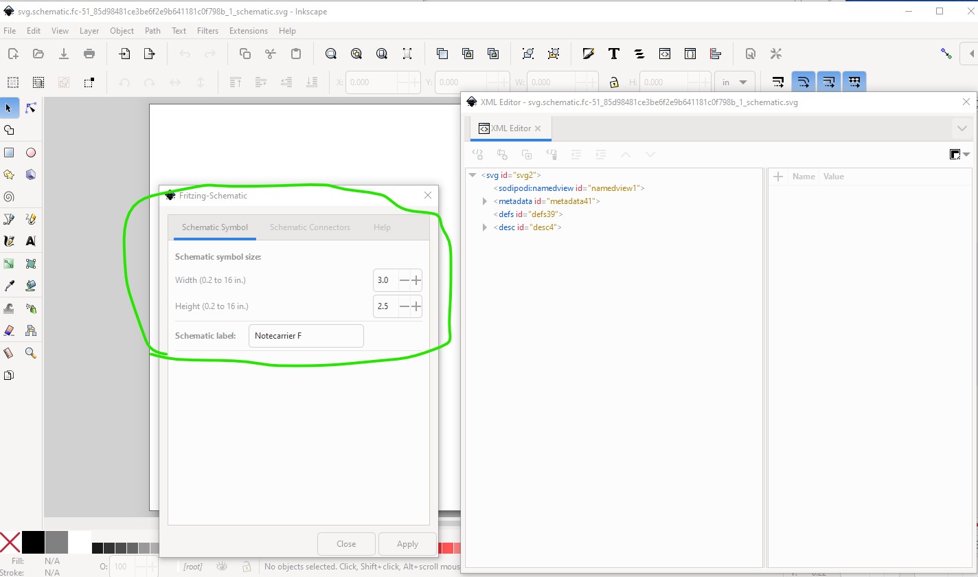
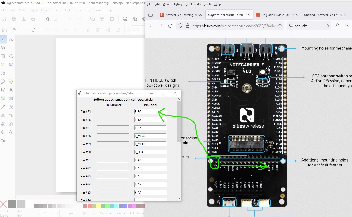
the height and width need to be set to 1 plus the number of connectors times 0.1in. In this case left and right have 24 pins so height needs to be 2.5in and the bottom has 28 connectors and needs to be 2.9in minimum, set to 3.2 inches to provide for a space between connectors. The Schematic label box needs the name of the part Notecarrier F in this case) Now we move on to setting the number of pins in each edge like this
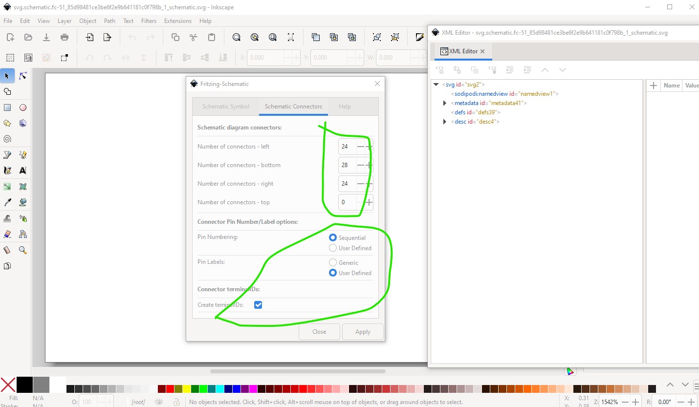
here we set left to 24 pins bottom to 28 pins right to 24 pins and top to 0pins. You want to set the bottom settings (which I think is the default) as listed then click apply to start the extension. That brings up this
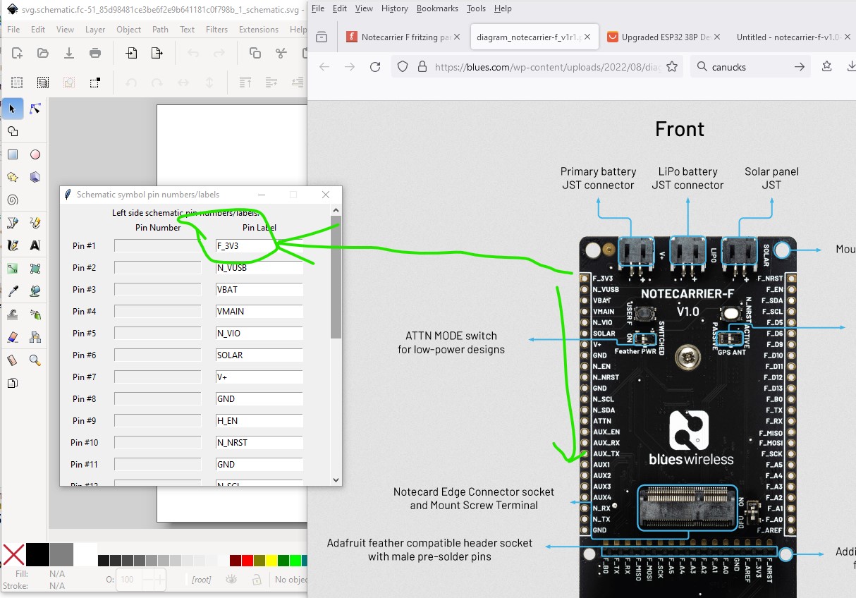
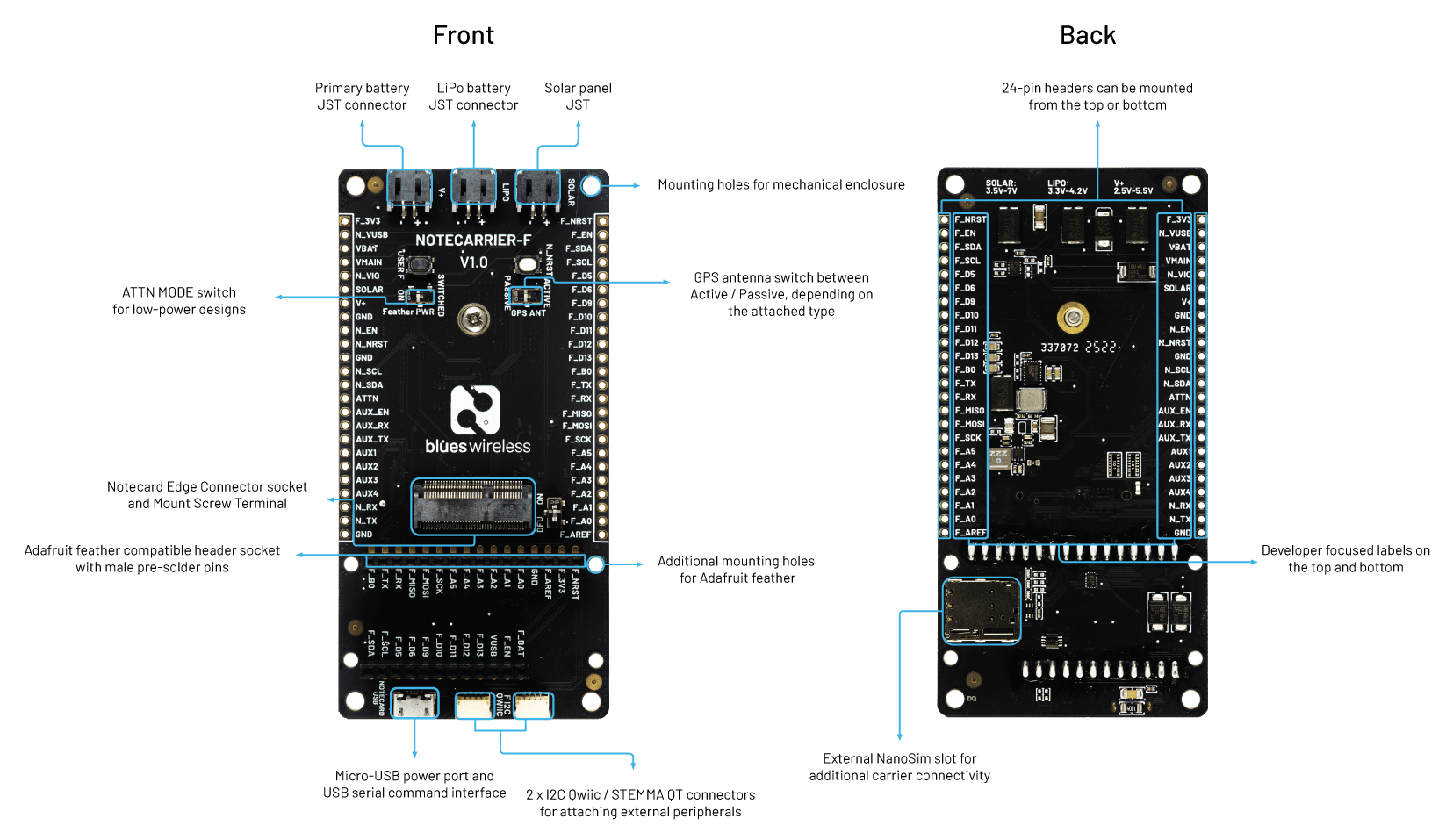
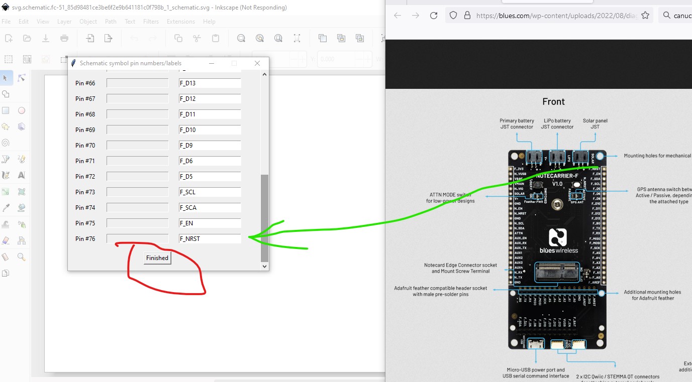
Here we want to set the pin labels according to the text on the pcb
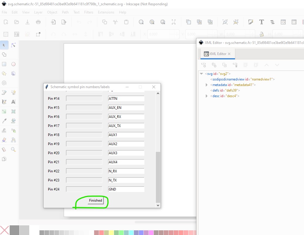
when finished (and checked!) click finished and it will move to the bottom pins.
fill in the pin names
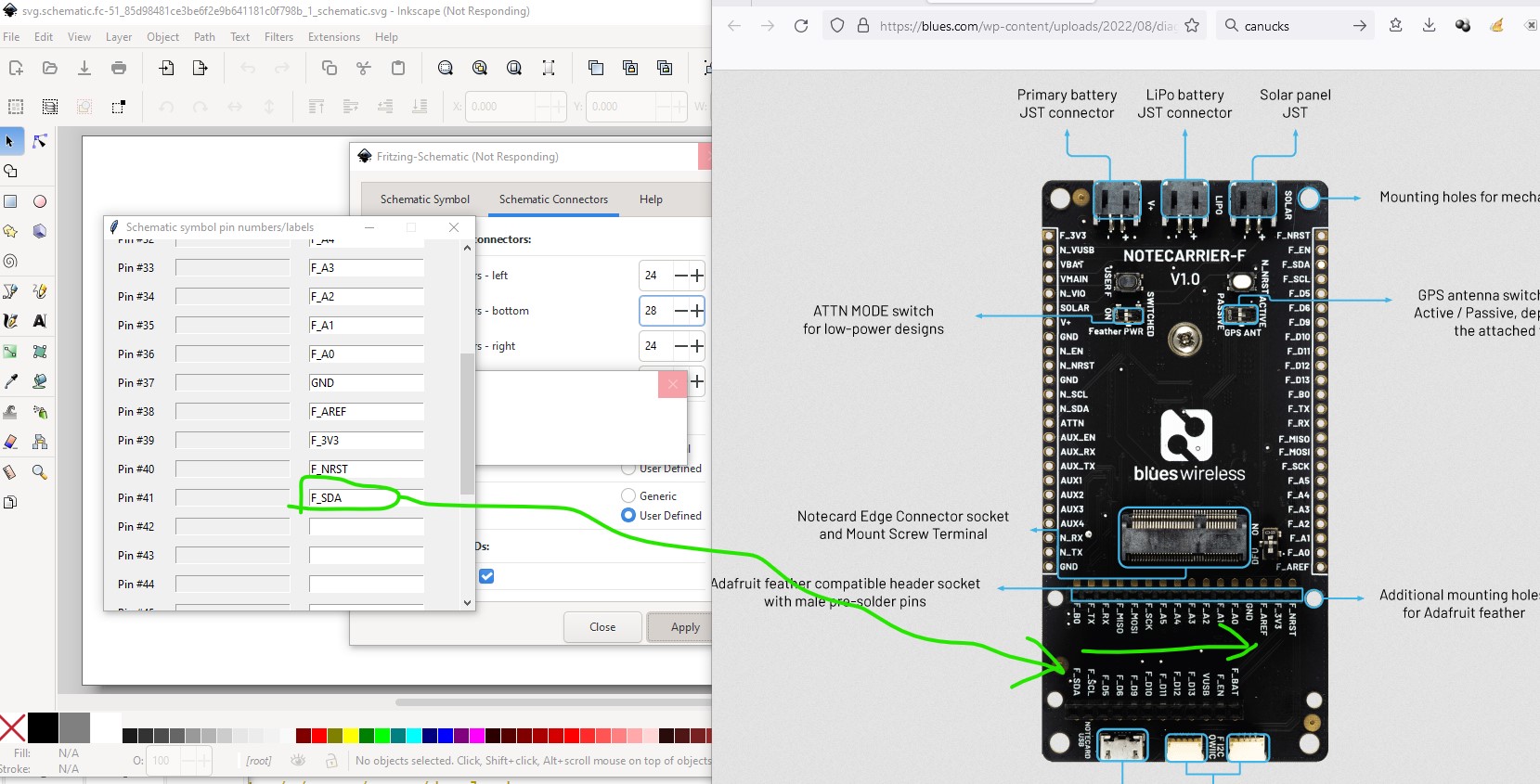
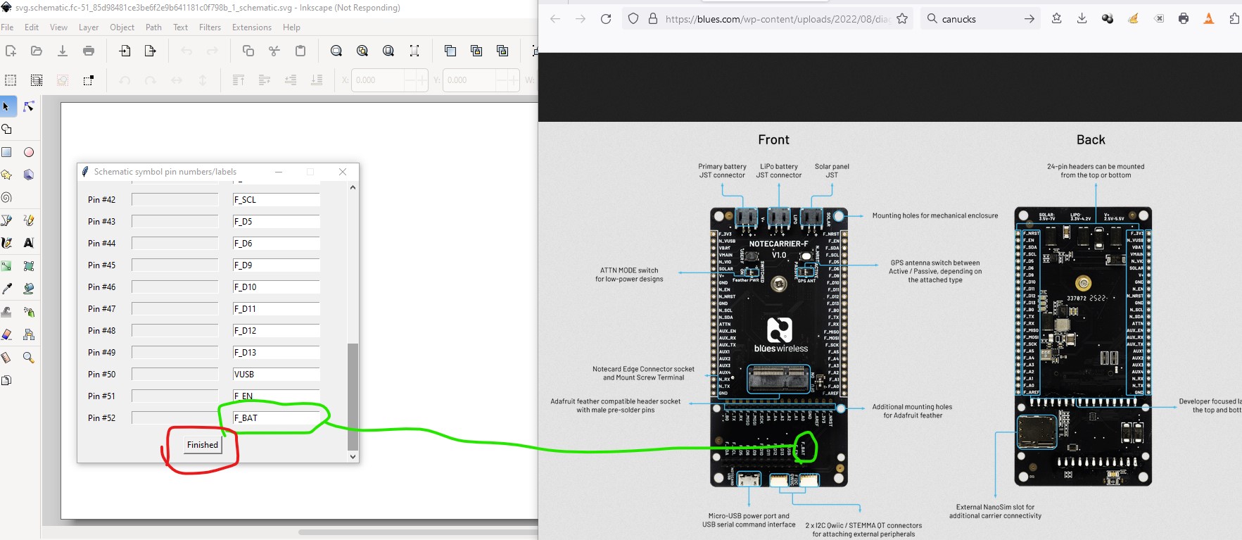
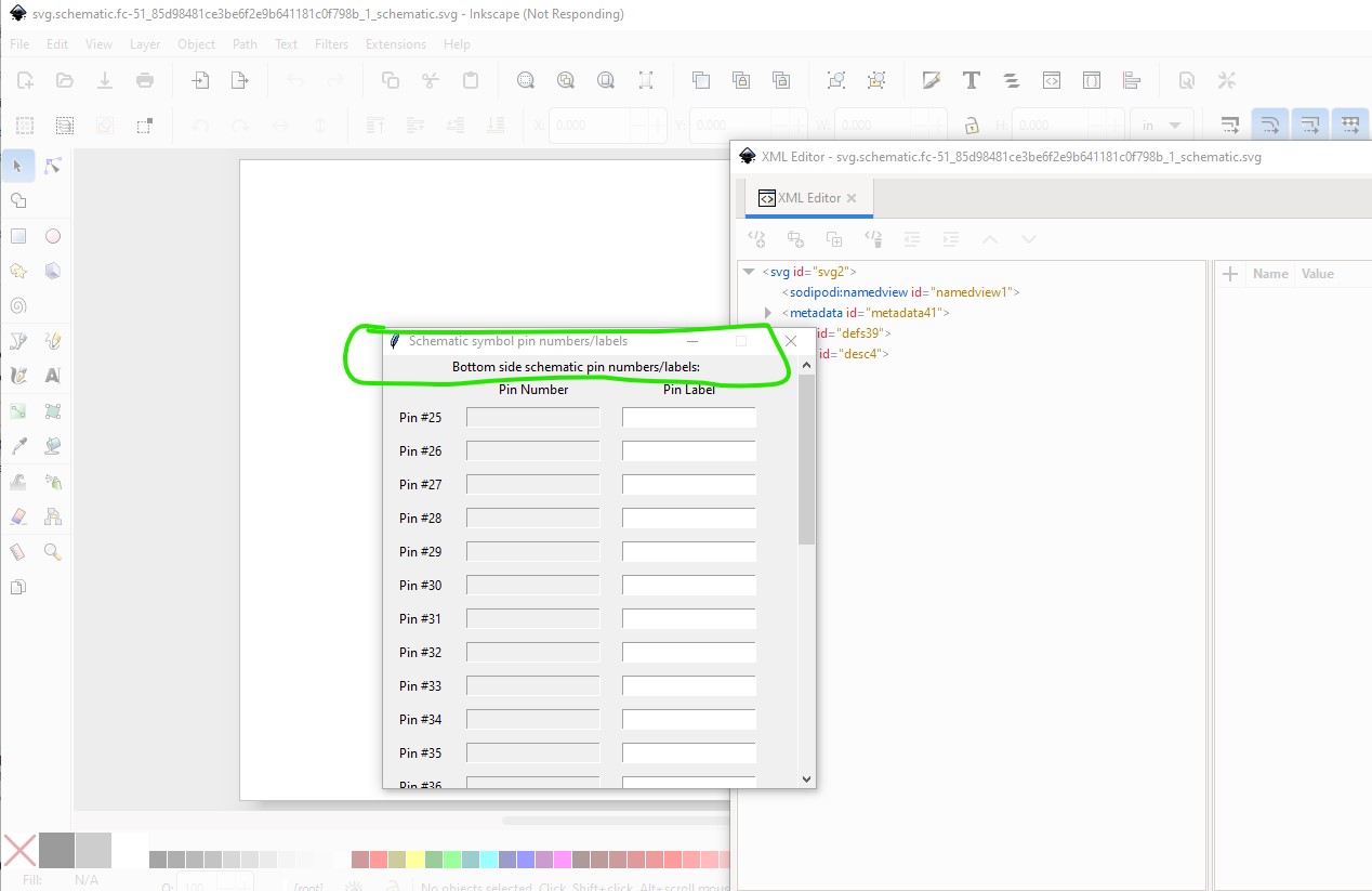
then check them and press finished to move on to the right connector.
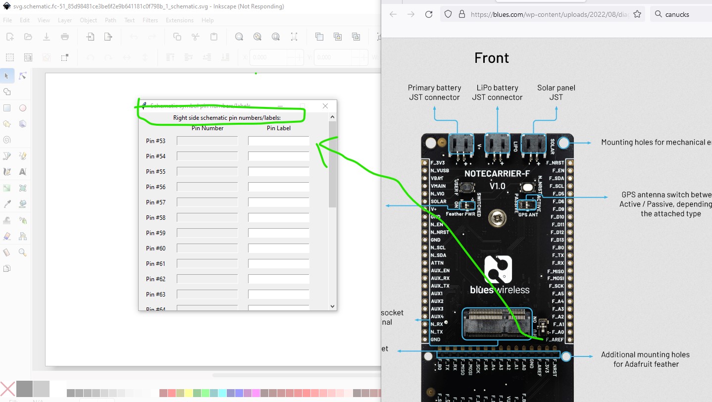
pressing finished here will then create the schematic svg
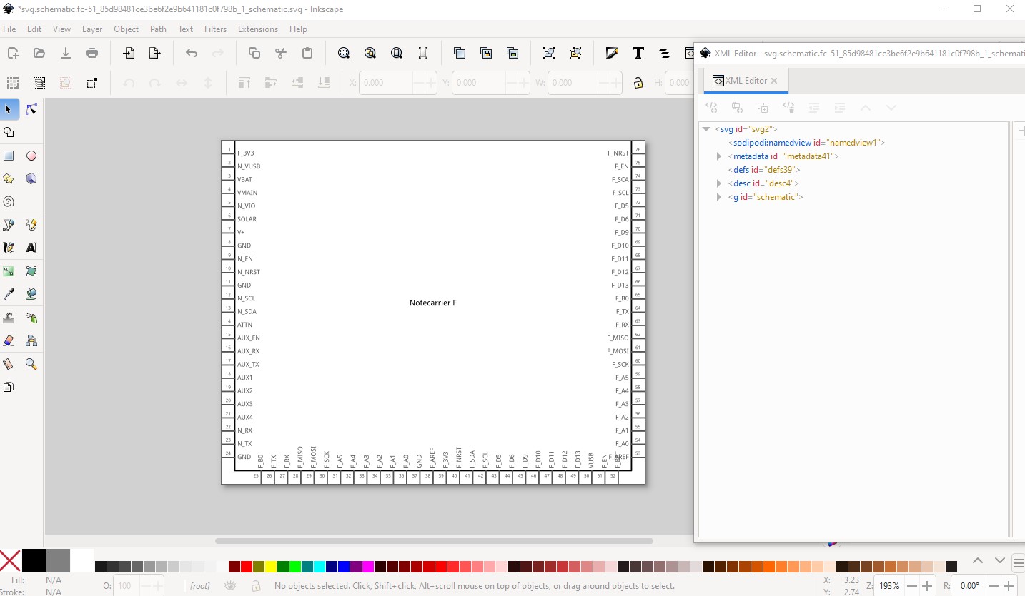
this one is a little too small so ungroup the svg
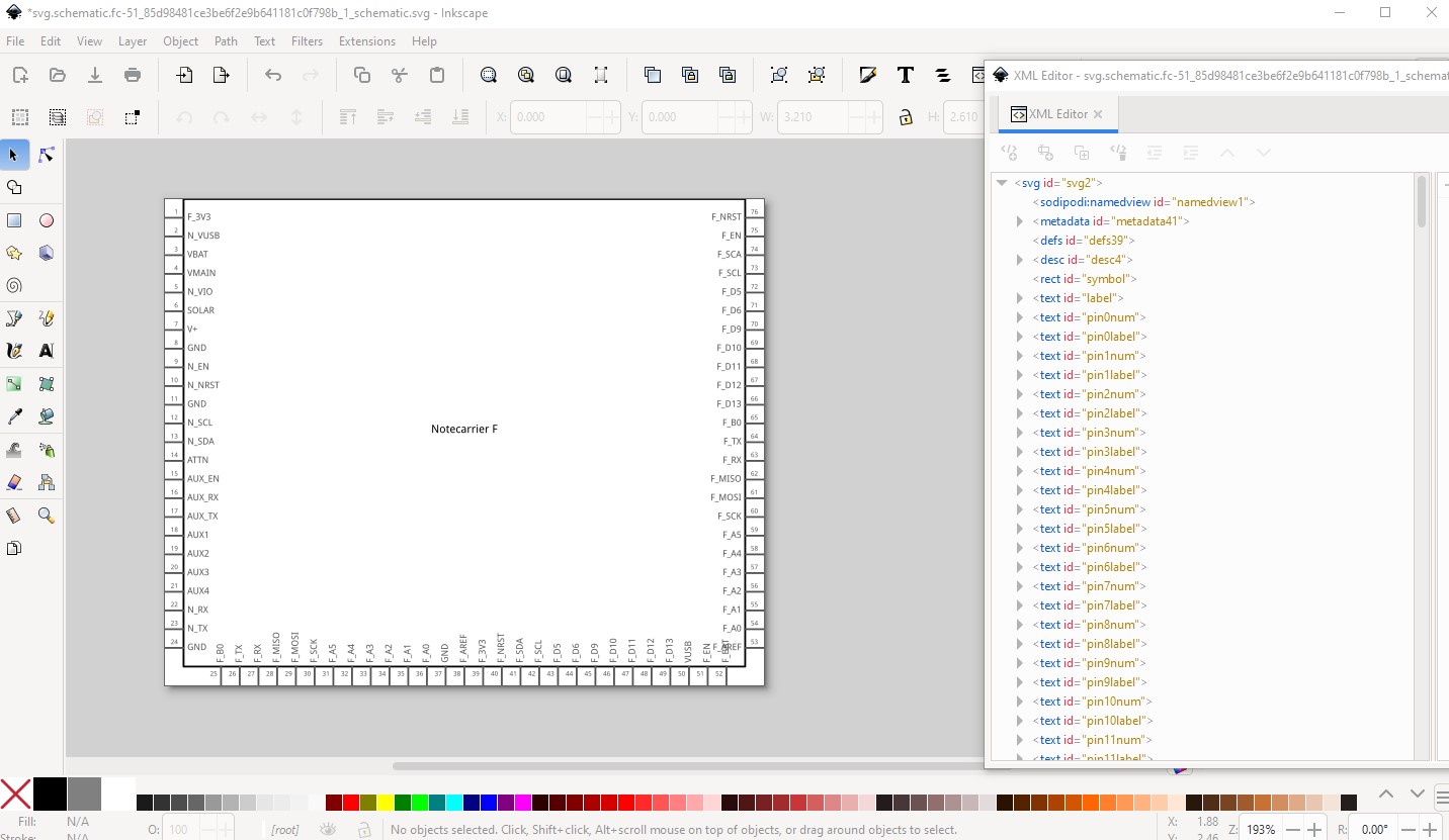
and select and move (in 0.1in intervals by clicking the x and/or y increase/decrease bars in the tool bar (making sure dimension is set to inches!) to move things in to position.
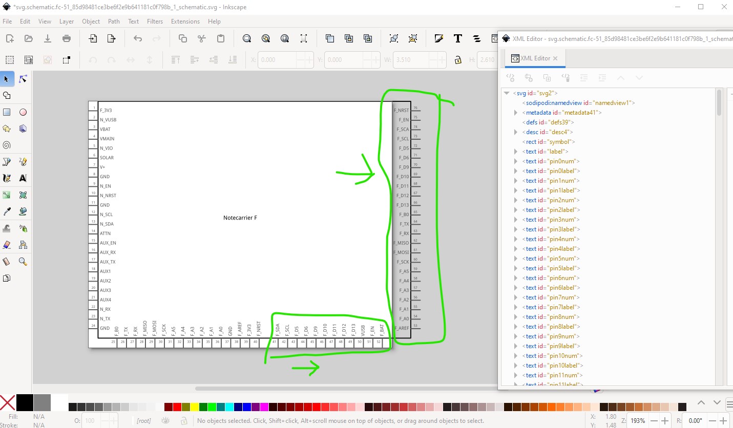
Note I added a space to separate the two bottom connectors from each other.
then do edit–select all, edit->resize page to selection and object->group and rename the group to schematic to set the layerId and then save the svg as plain svg. Now both breadboard and schematic are complete. The breadboard svg needed further modifications because of both the missing connector (which I didn’t find til schematic) and because the text tspans are configured oddly and deleted all the text when setbb.py ran. I manually replaced all the text with standard non tspan text and things were then fine (if you compare your original svg to the one in the fzpz file, unzip the file to get it, you will see the changes I made.) With both the svgs completed we now only need an fzp file to complete the part. I started from a template .fzp file that has no connectors. So first I needed to create a connector file by doing
cons.py -n -p cons 76
(the file name cons in the tutorial is different but it works the same!) which creates a file that looks like this:
      <connector id="connector0" type="male" name="Pin 1">
        <description></description>
        <views>
          <breadboardView>
            <p svgId="connector0pin" layer="breadboard"/>
          </breadboardView>
          <schematicView>
            <p svgId="connector0pin" layer="schematic" terminalId="connector0terminal"/>
          </schematicView>
        </views>
      </connector>
      <connector id="connector1" type="male" name="Pin 2">
        <description></description>
        <views>
          <breadboardView>
            <p svgId="connector1pin" layer="breadboard"/>
          </breadboardView>
          <schematicView>
            <p svgId="connector1pin" layer="schematic" terminalId="connector1terminal"/>
...
This gets copied in to the fzp file and then the pin names (I usually use the schematic svg to set them, but a pinout map will also work) to set the description fields to the pin names. To suppress the pcb view you need to change this
    <pcbView>
      <layers image="pcb/notecarrier_f_1_pcb.svg">
        <layer layerId="silkscreen"/>
        <layer layerId="copper0"/>
        <layer layerId="copper1"/>
      </layers>
    </pcbView>
to this
    <pcbView>
      <layers image="breadboard/notecarrier_f_1_breadboard.svg">
        <layer layerId="breadboard"/>
      </layers>
    </pcbView>
which reuses breadboard for pcb which will suppress pcb view. In addition I needed to set the bus values which creates this
which associates pins which have an internal connection in to the same group. There are a lot of them in this board. They are set like this
    <bus id="F_3V3">
      <nodeMember connectorId="connector0"/>
      <nodeMember connectorId="connector38"/>
    </bus>
    <bus id="GND">
      <nodeMember connectorId="connector7"/>
      <nodeMember connectorId="connector23"/>
      <nodeMember connectorId="connector36"/>
    </bus>
    <bus id="F_B0">
      <nodeMember connectorId="connector24"/>
      <nodeMember connectorId="connector64"/>
    </bus>
in the fzp file. With that the part is complete and it needs to be run through FritzingCheckPart.py to make sure it is correct. Hopefully I haven’t scared you off from making parts, you have most of the skills needed to do so and experience making parts helps.
Peter
1 Like
Hello Peter, Thank you. And no, you didn’t. I’m even more eager. I’ll follow up to correct this.