This one is a Fritzing quirk. The problem is that you have px in the font-size. To fix this you can either run the part through FritzingCheckPart.py (which will automatically fix this) or probably easier in the short term, edit all you svgs with a text editor and do a global remove of the px in the file like this:
  <g id="schematic">
    <rect fill="none" height="6500.0" width="2000.0" stroke-width="10" stroke="#000000" stroke-linejoin="round" stroke-linecap="round" id="symbol" x="105" y="105"/>
    <text x="1105" y="3355" font-family="'Droid Sans'" font-size="60px" fill="#000000" id="label" text-anchor="middle">NALoadCenter</text>
    <text x="75" y="1185" text-anchor="end" font-family="Droid Sans" font-size="35" fill="#555555" id="pin0num">1</text>
    <text x="125" y="1217" text-anchor="start" font-family="'Droid Sans'" font-size="49px" fill="#555555" id="pin0label">Ground</text>
This "font-size=“60px” is a problem and most svg editors add the px for CSS compliance which causes the fault in Fritzing (I’m hoping to get a fix for this, there is a discussion on this in another thread here:
Edit Breadboard Icon Failed - #16 by vanepp
with one of the developers, so I have some hope he may find a fix. Until then either FritzingCheckPart.py or a global replace of “px” with “” in a text editor should fix this (there may be cases where it won’t but I have not yet run in to one!) Suppressing pcb view again requires a text editor, you need to edit the .fzp file (in your case this one)
part.NAGenericUtilityPanel001_7566471799b70f70a61f5a80b7c1c3ee_34.fzp
and replace this
    <pcbView>
      <layers image="pcb/NAGenericUtilityPanel001_f4e5e973aa4b719c30a1aa0d470b17e1_43_pcb.svg">
        <layer layerId="copper1"/>
        <layer layerId="silkscreen"/>
      </layers>
    </pcbView>
with this from here (earlier in the file)
    <breadboardView>
      <layers image="breadboard/NAGenericUtilityPanel001_f4e5e973aa4b719c30a1aa0d470b17e1_43_breadboard.svg">
        <layer layerId="breadboard"/>
      </layers>
    </breadboardView>
but with only part of it which will reuse the breadboard view as pcb, As far as I know parts editor can’t do this only editing the fzp file directly, but it has the effect of making pcb view a blank (as Fritzing requires something to render in pcb view, but knows that breadboard is the wrong layerId and thus doesn’t render it but is happy it has something render!)
      <layers image="breadboard/NAGenericUtilityPanel001_f4e5e973aa4b719c30a1aa0d470b17e1_43_breadboard.svg">
        <layer layerId="breadboard"/>
to give this:
    <pcbView>
      <layers image="breadboard/NAGenericUtilityPanel001_f4e5e973aa4b719c30a1aa0d470b17e1_43_breadboard.svg">
        <layer layerId="breadboard"/>
      </layers>
    </pcbView>
Those two should fix all your issues I think. The px problem works the same in breadboard, so it needs to be done there too.
Yes, because by default snap to grid is enabled and the wires will snap to the 0.1in grid (which is the default) so in breadboard and schematic your parts need to align to the grid (i.e. the elements need to be 0.1in apart) to align correctly with other parts. You will notice the generated schematic aligns on exactly 0.1in boundaries. It looks like you have a copy of FritzingCheckPart.py, so if you use the svgs it wrote (the originals are in the .bak files) they should work correctly if the pin alignment is correct (FritzingCheckPart won’t adjust the pin spacing.) It should remove all the px from the font-size and stop the large text. The pin offset in schematic is an extension quirk, it can be fixed in two ways: reduce the size of the height of the svg in the extension so it is shorter (so the pins are on the same level) or what is probably easier, is edit the svg from this

first ungroup the svg so you can easily move things (at least in Inkscape!)
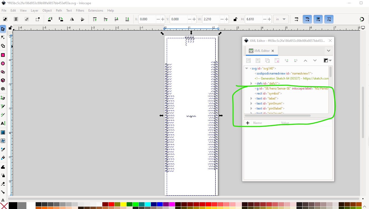
then use the tool bar to move the left side up in 0.1in increments to the new position.

Do the same to the right side.

then reduce the height of the rectangle to make the schematic smaller (which is desirable!)

then do an Edit->select all and Edit->resize page to selection to reset the viewbox and an Object->group to re make the layerId group and name it schematic then save the svg as plain svg (I imagine your svg editor will have similar commands, hopefully one that moves by 0.1in increments or this gets very painful!) Hope this helps, if not feel free to ask!
Peter