You are missing the copper0 layer everywhere and thus won’t get through hole anywhere. The slots in the pads will also not render (Fritzing can’t do tabs, nor generally can the board houses.) This tutorial explains how to get mixed through hole and SMD parts (although it is painful assuming you are using Inkscape):
I read the topic… Yes, the different copper0 & copper1 is now old. I tried that too.
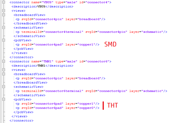
But, it’s not mandatory to keep the “same pin svg” with “same name” for THT.
Because, I create/edit part via part file (.fzp), and there, the svgId can be edited to different names for copper1 & copper0.
and for the smd pads only defines copper1 in the connetor but for the through hole portion defines both copper1 and copper0, which also works (as long as you don’t need different connections on different sides of the board in the same place.)
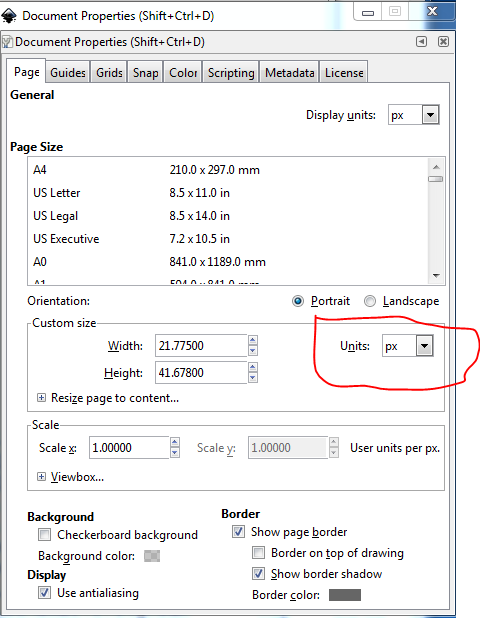
In all the svgs the Units should be in inches (in) not px. Px causes Fritzing to guess at the original resolution which it may or may not have gotten right this time. The result is that the scale may be incorrect making the pads the wrong size:
Actually, I edit in AI, with mm unit.
And, yes, while editing core svg, AI detects the values as “mm”, and I have to converted them to mil-inch manually…!!
Yes, AI saves the xml like that, what unit I currently using or something… But never had a problem with that…
Anyway I missed the main problem with SMD…
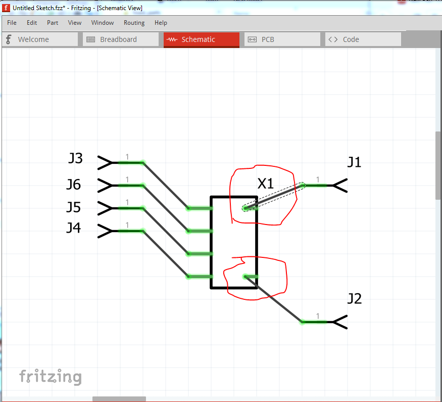
They all working smoothly if I use the parts on TOP layer of the PCB.
But, whenever I move it on the bottom layer, the SMD pads still connecting with TOP layer trace…!!!
Not only my parts, even the core parts…
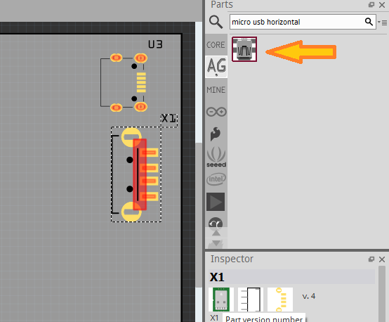
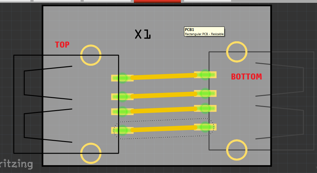
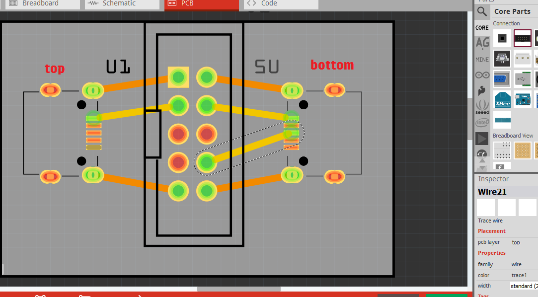
Here, a screenshot with same part (sparkfun usb connector) on different layer connected with TOP traces…
Maybe it’s a creation Failure…!!!
Before I got distracted in to the display obsolete part issue that I just fixed, I had though of this and was about to try your part on the bottom of a board. You likely need completely separate copper1 and copper0 groups (not copper1 as a subgroup of copper0 which I think is the current configuration.) The SMD pads need to be only in copper1 and the through hole pads need to be in both. Then I think swap top to bottom may work correctly because copper1 will be as Fritzing expects it. Luckily for me you found the problem first so I don’t have to poke at it.
I tried a lot with many ways… But It didn’t work…!!
And, my conclusion is THT & SMD in a single part is impossible till now…
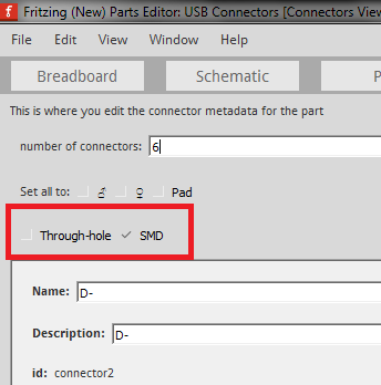
Because, Fritzing only supports either “Through-hole” or “SMD”, as per as the part editor options…!!
But, I separately created only a PCB view terminal, but can’t make it as jumper without schematic…!!! 187. Terminal (USB-A Male) 1.fzpz (2.9 KB)
I’m not clear what you are trying to create in the above .fzpz, but it isn’t properly configured. Schematic and breadboard likely don’t understand copper1 and copper0 layers and thus don’t render them. If you post the .fzpz file for your complete (if not working) part two posts back, so I can see what you are trying to achieve, I’ll have a bash at doing it for you although you may be correct that it isn’t possible to make it work completely.

 so I don’t have to poke at it.