I have created a PCB design and Fritzing is stating through the autorouting that Vin should be tied to GND and 5V should be tied to GND. However, I do not believe this is correct. Is this a bug?
SeniordesignV3 - Copy.fzz (38.8 KB)
I have created a PCB design and Fritzing is stating through the autorouting that Vin should be tied to GND and 5V should be tied to GND. However, I do not believe this is correct. Is this a bug?
SeniordesignV3 - Copy.fzz (38.8 KB)
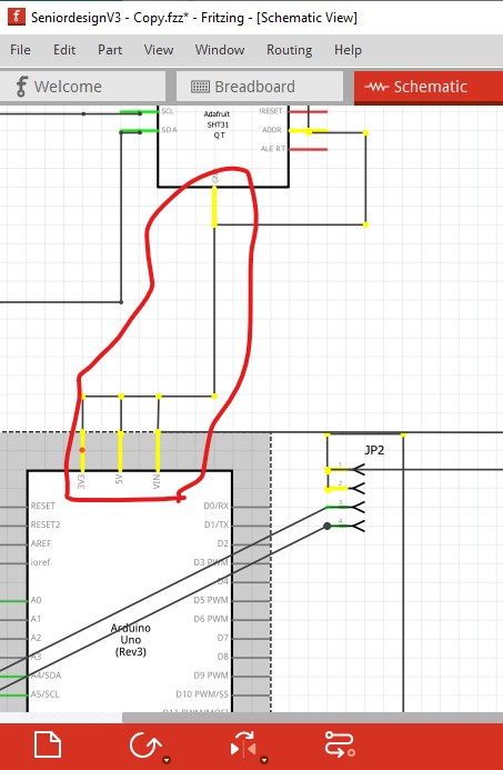
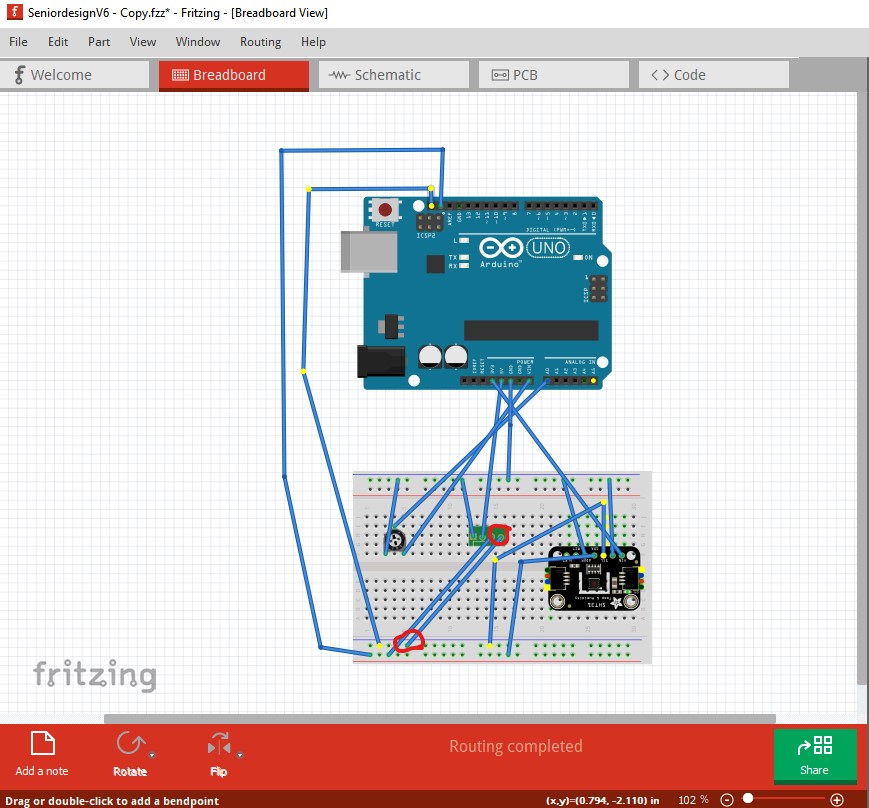
Yes it is incorrect, no it is not a bug. You have shorted 3.3V, 5V, VIn and ground in schematic. That reflects in to both breadboard and pcb views causing the errors you are seeing. Here I clicked on the 3.3V pin in schematic and as you see the 5V, Vin and GND pins also light up yellow indicating they are all shorted together. This reflects as rats nest lines (as a short between the wires that has not yet been routed) in both breadboard and pcb views. I deleted all traces in schematic (which is wrong anyway) then all traces in pcb (via routing->Select all traces, then hit the delete key in both views) and then ran autorouter again and it appears to create a correct routing in pcb. So you likely only need to click on the rats nest lines in schematic and route the connections (carefully so as not to introduce shorts!) as it appears breadboard may be correct (you need to verify the resulting layout is correct though!)
edit:
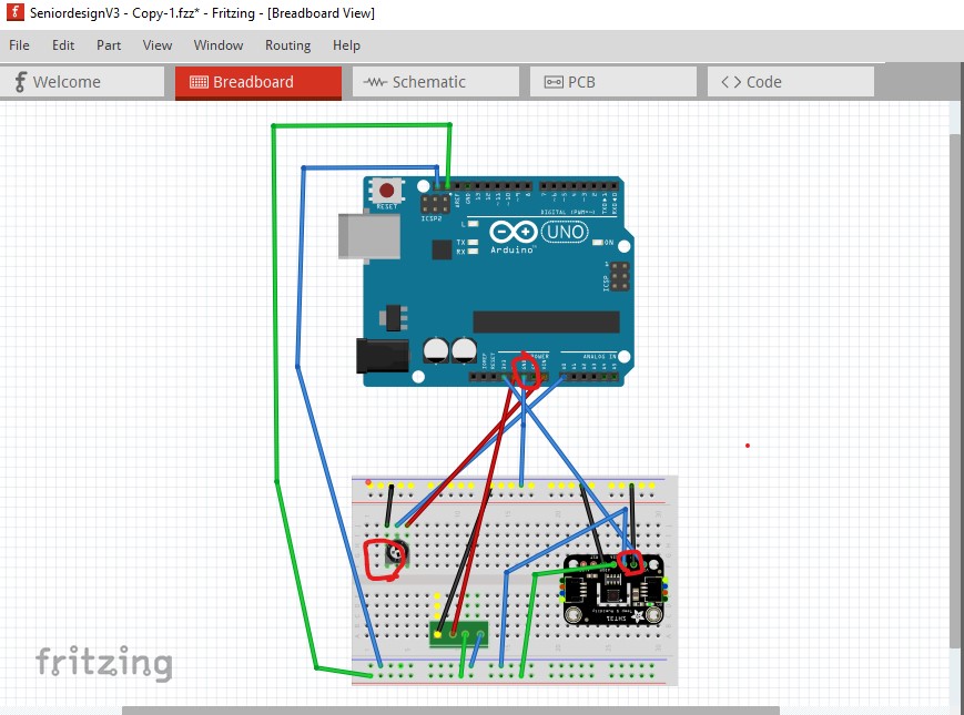
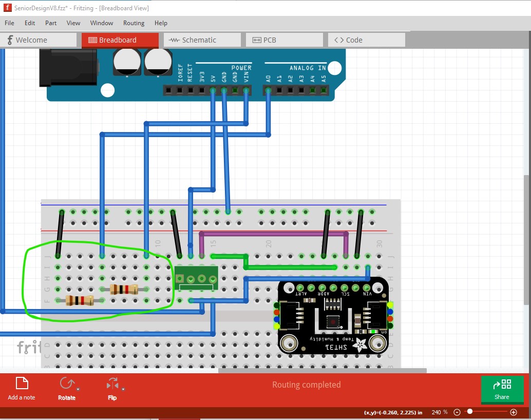
There are also problems in breadboard: you need to enable align to grid
then likely move all the components so they snap to the grid. At present there are a number of the grounds (and likely other connections) not connected correctly.
again I clicked on a ground wire and not all the ground connections (specifically the three outlined in red above) are connected all expected connections should light up yellow, the ones that do not are not connected. You need to move the wires til they connect correctly before autorouting will work correctly. Note I deleted all traces in both schematic and pcb before doing this in breadboard view.
Peter
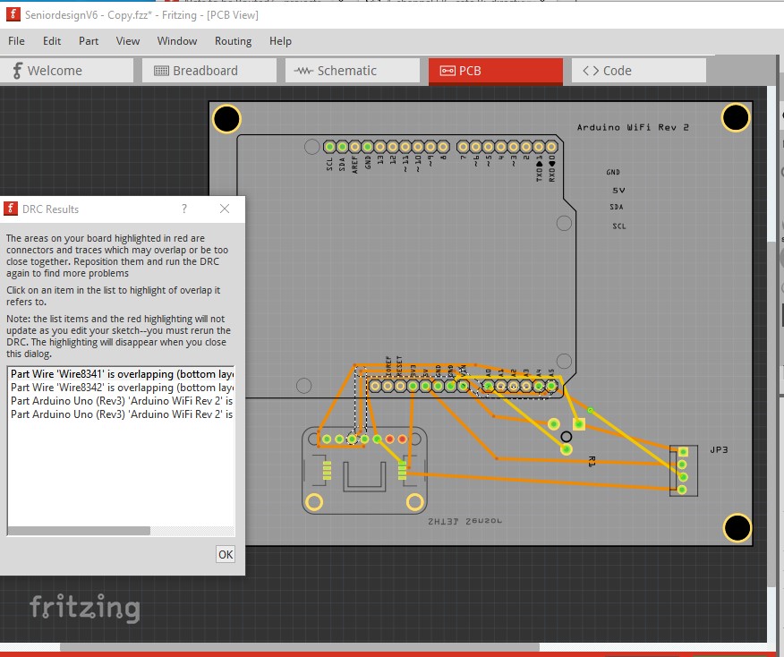
All the information above was excellent! I appreciate your help. I am now having issues with pin 3 and pin 4 on the 4 pin header not wanting to connect on the schematic and PCB. Any advice?
SeniordesignV6 - Copy.fzz (36.4 KB)
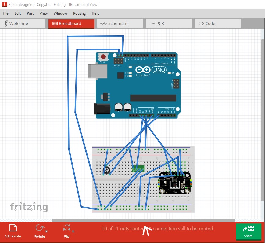
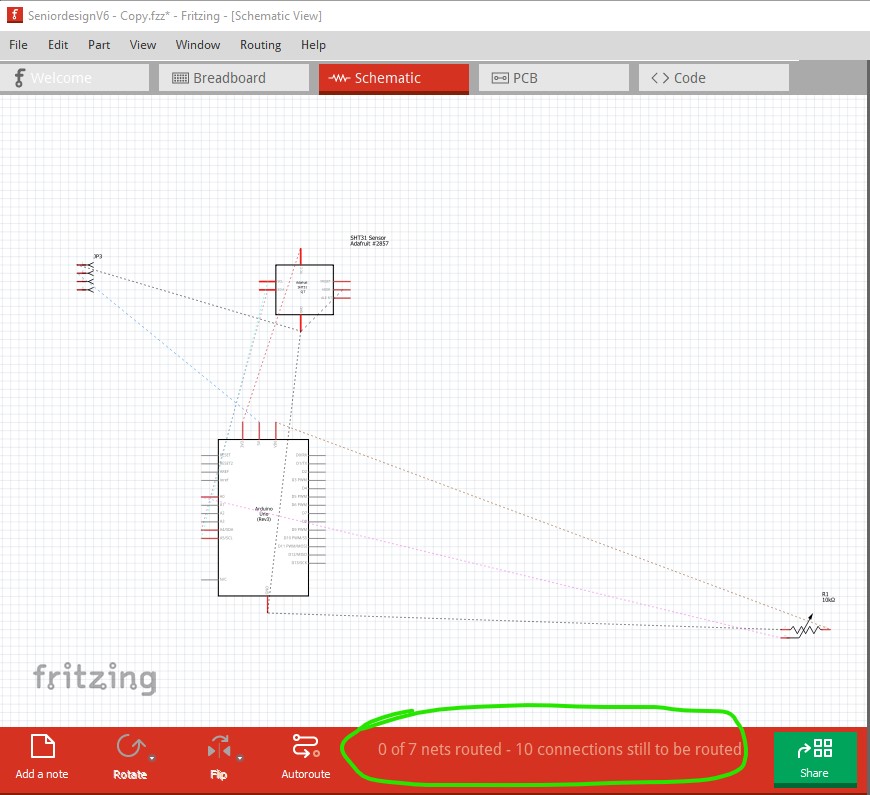
Clicking on the 10 of 11 nets routed (which should be routing complete) should show the unrouted net in yellow.
but instead shows this (which is wrong, indicating there is an error in one of the other views)
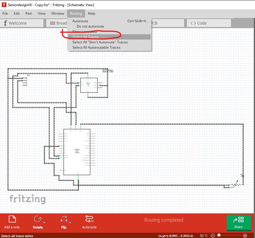
so change to schematic and delete all traces.
then hit the delete key to delete all the traces.
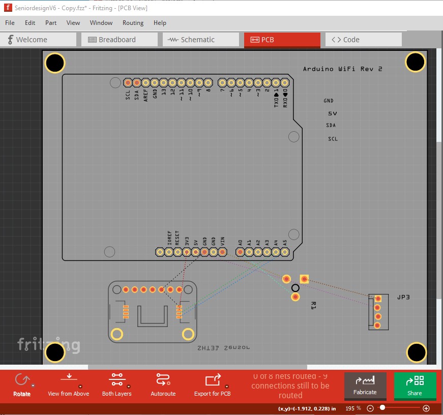
at this point it shows 0 of 7 known networks routed as it should (the 7 networks may be wrong as we haven’t deleted pcb yet though!) So change to pcb and do the same thing. Note it currently says routing completed at the bottom of the screen.
now hit the delete key to delete all traces.
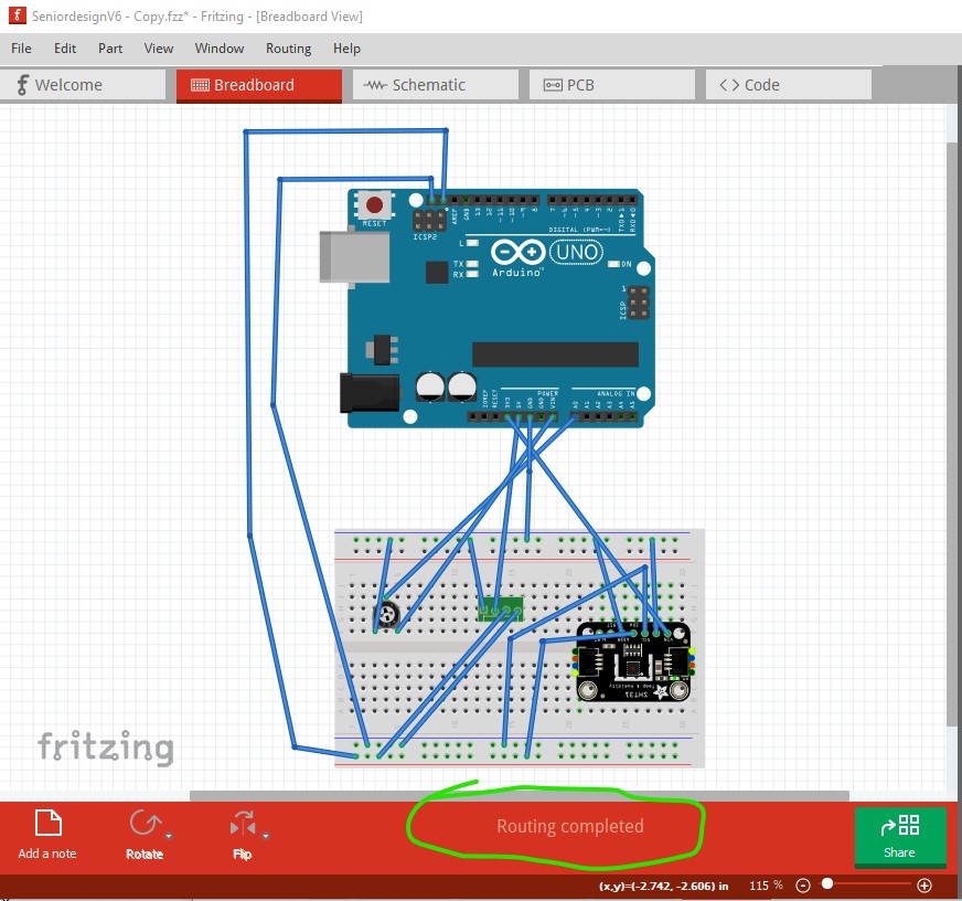
Now we get 0 of 7 nets routed as we should and breadboard shows routing complete (so there was a conflict in one of the other views.)
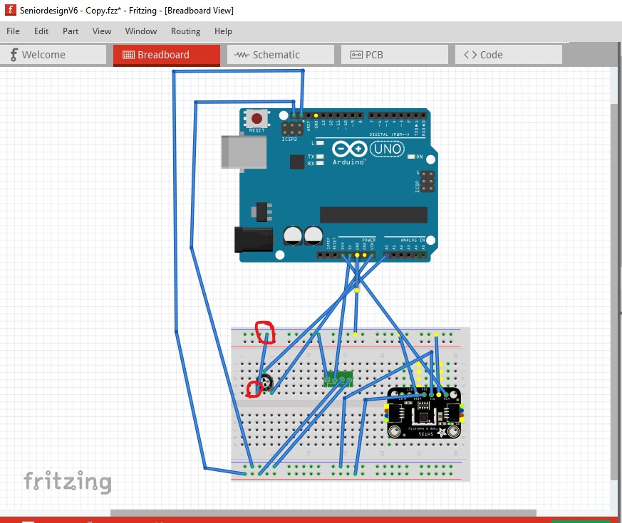
While it shows routing complete (because all the nets it thinks are connected are routed!) that is still not correct. There are 3 connections missing.
here the SDA net is missing the connection to the 4 pin header (the wires appear connected but don’t light yellow indicating a valid connection!) Same with the SCL connection, it doesn’t connect to the 4 pin header (and thus won’t show up in schematic or pcb as a connection.)
And finally the ground connection to the pot is also missing.
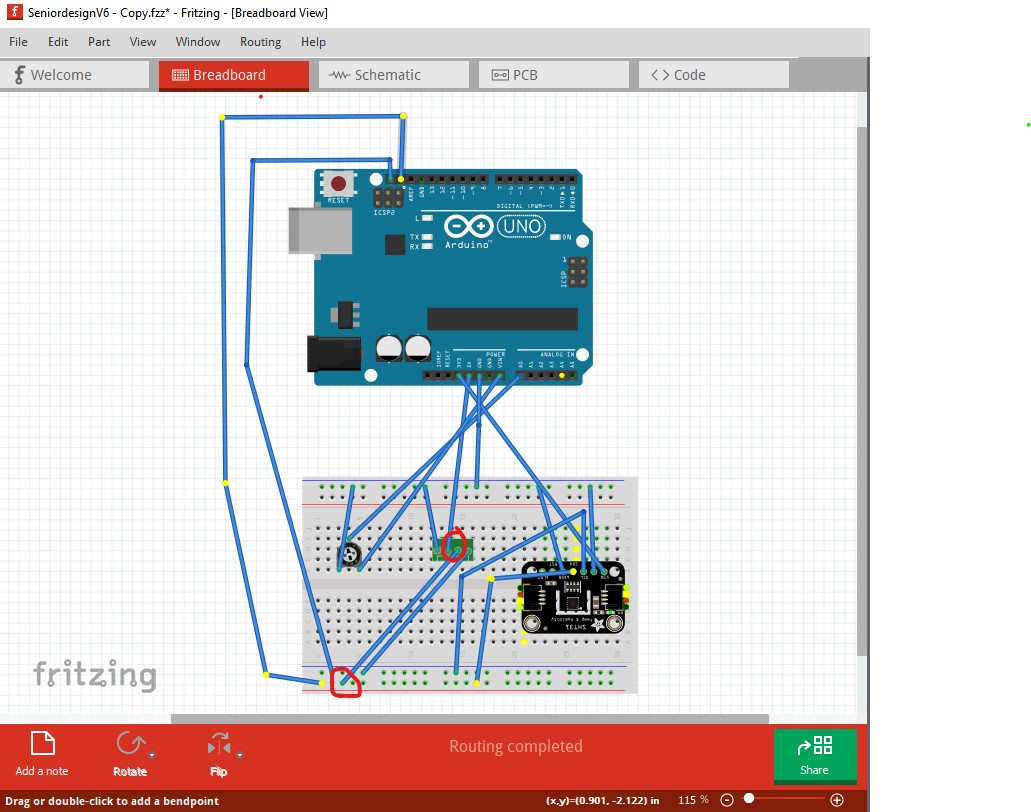
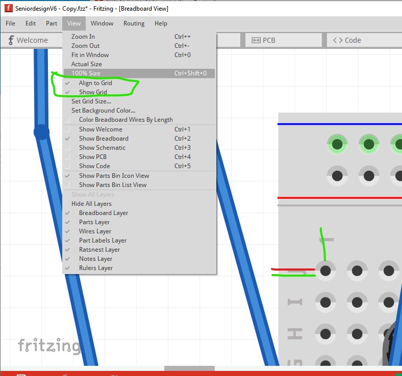
So first we need to fix all these problems. So start with enabling Align to grid (which is on by default, so you must have disabled it at some point, which is a bad thing to do in breadboard!)
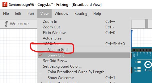
so set align to grid (which won’t take effect until we move all the parts!)
Note the breadboard holes do not currently align to the grid. They are slightly offset in y from the grid (the red line is the center of the pin the green is the grid.) Clicking on the breadboard and moving it slightly in x and y will cause it to snap to the grid.
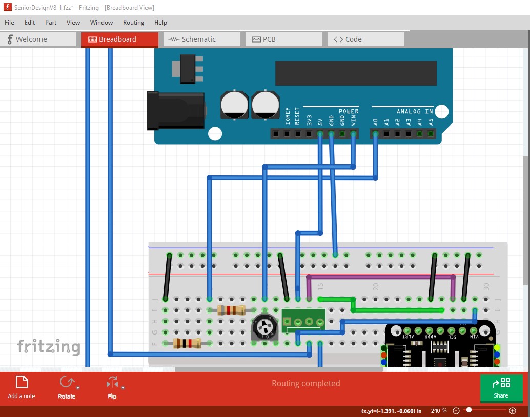
Now move the pot a couple of positions along in X. Note that its 3 connections to the breadboard are green indicating they have connected to the breadboard as are the three wires that were going to the pot.
now move the pot back to the wires (note I also moved the wires so they connect to the breadboard as they have to in real life rather than the pins on the part!) I also changed the color and positioning of the wires to make the connections clearer and as short as possible. Now when I click on any ground pin all the grounds light up yellow:
As do all the other pins. I’ll note in passing, that the pot connecting to Vin (typically 6 to 9V) with the wiper going to the A0 pin is dangerous because the A0 pin is limited to 5V in (and thus the top of the pot should more likely connect to 5V!) As well you need a level translator from 5V to 3.3V (such as this adafruit device
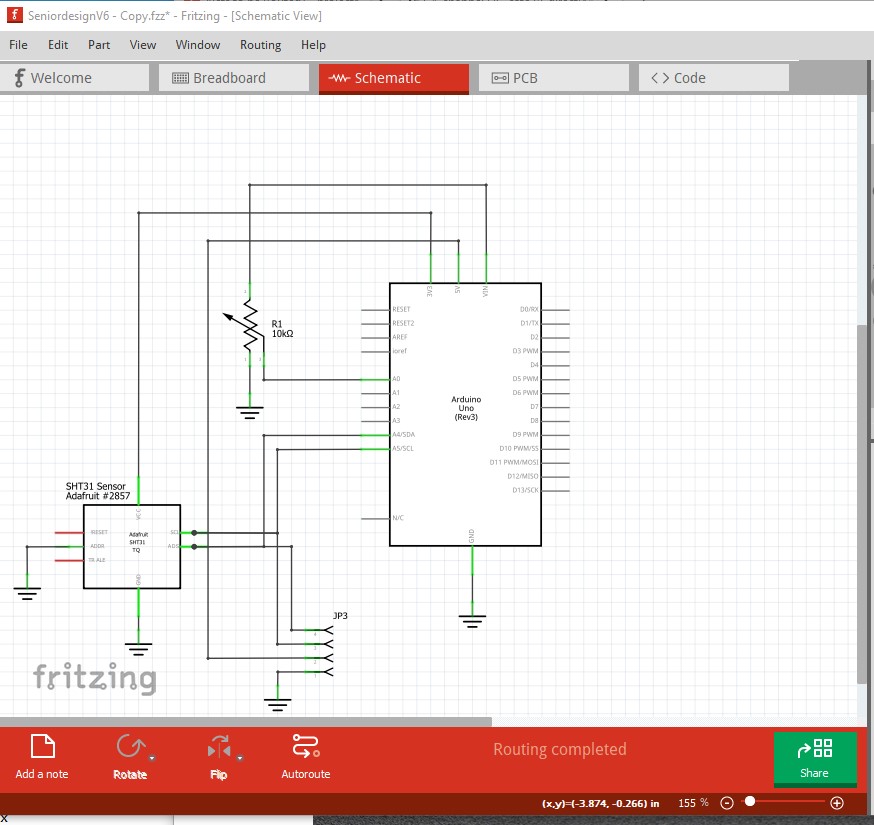
on the SCL and SDA lines to protect the 3.3V inputs of the SHT31 sensor or change to a 3.3V Nano instead of the current 5V Uno. At this point breadboard appears to be correct and routing is complete so now we move on to schematic. First move the components around until the routing looks correct, then click on the rats nest lines one at a time (to route them) then move the wires in to a sensible position until routing is complete:
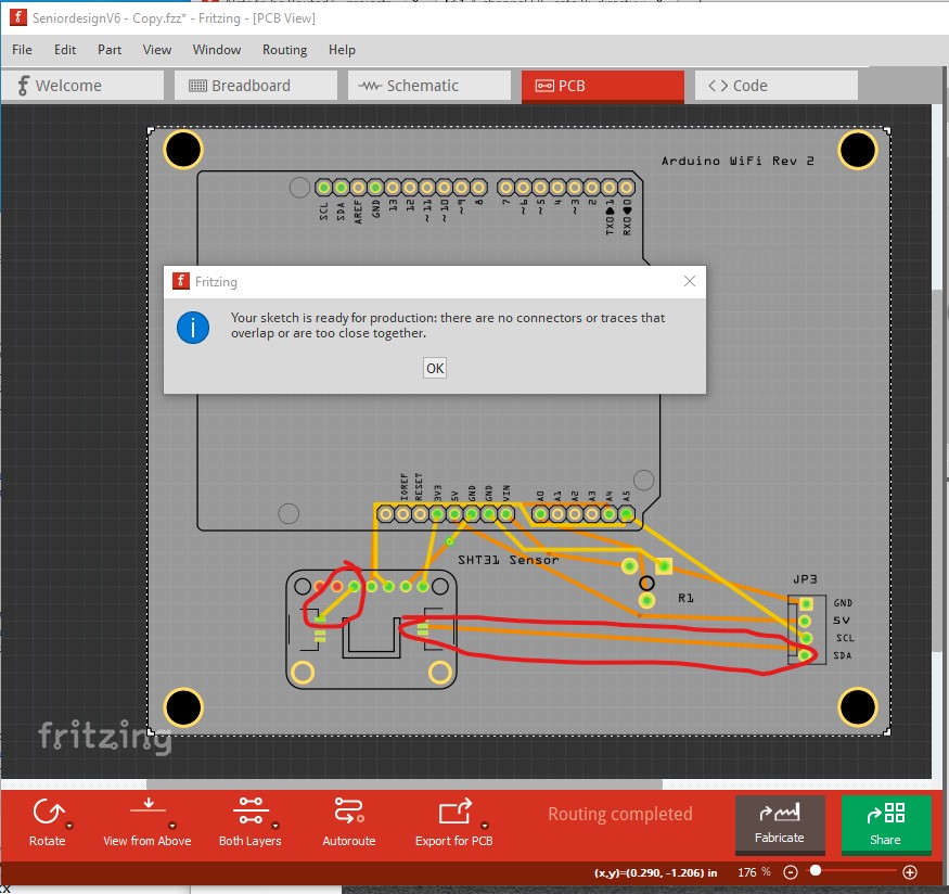
then move on to pcb and autoroute it. As usual autoroute does a poor job (it doesn’t pass DRC for instance)
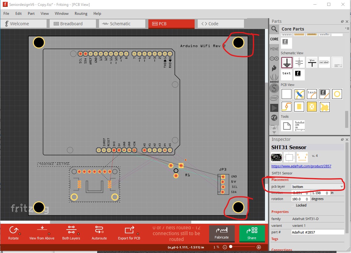
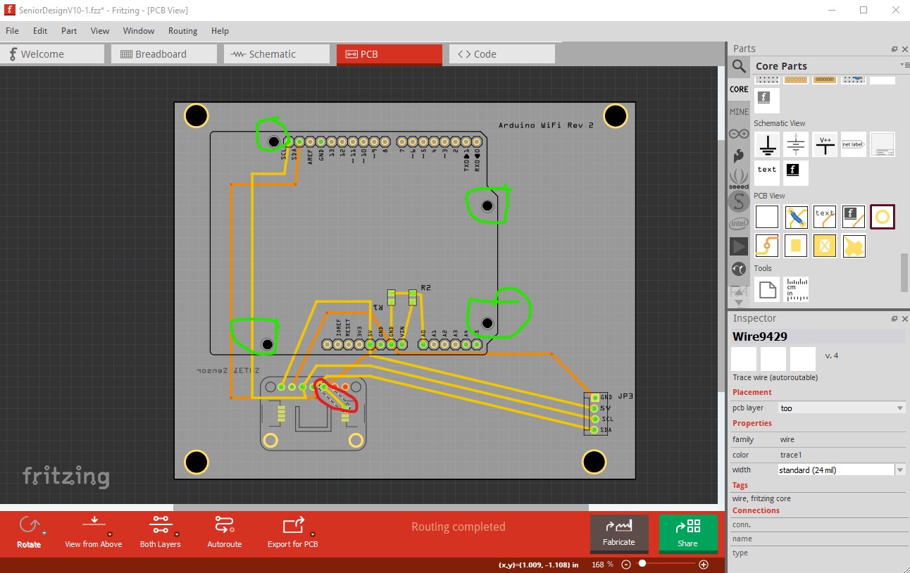
For some reason the SH31 is on the bottom of the pcb rather than the top. I assumed this is an error and moved it to the top of the pcb. The holes for the mounts are outside the pcb area (and will thus be truncated and are thus likely incorrect and need to be moved) The labels for the header were in the wrong place.
When I autoroute that it works and passes DRC, but is likely not optimal as it is making connections to the SMD pads which are likely not accessable on the part (as they appear to be SMD connectors.)
So delete all the traces and manually route the board. Which procduces this which likely will do what you need.
which comes from this sketch
SeniordesignV6 - Copy-fixed.fzz (36.9 KB)
Peter
Hey Peter,
Thank you for all this information. I did want the sensor on the bottom as I am wanting the Arduino on top of the PCB, the PCB next, and then the sensor on the bottom. In other words, the PCB will be in the middle of the sensor and Arduino.
In regards to holes for mounting, I want to put holes to mount the PCB, but you said they are outside of the PCB area. Can you further explain?
Lastly, I am using an Arduino WiFi Rev 2 board, which has SCL and SDA on the other side instead of configuring A4 and A5 as SCL and SDA for Arduino Rev 3. Should my SCL and SDA be routed to the other side then?
Looks like I screwed up and moved the mounting holes outside the board path when I changed something, as the mounting holes are in the correct place in your original sketch so disregard that part of the post. The need for a I2C level translator still exists however as the Arduino WiFi Rev 2 operates at 5V and the sensor is at 3.3V. It will probably work as it stands, but it is straining the sensor by applying 5V to a 3.3V input and may eventually cause it to fail.
Then you should swap in the Arduino WiFi Rev 2 from this post (which I just updated to be correct which it wasn’t.) Here the SCL/SDA lines are uncoupled from A4/A5 so they will route to the correct pins. If you delete the Uno with delete minus (rather than delete) Fritzing will leave the traces in place when deleting the part. You then need to drag the end of the traces to remake the connections after placing the Arduino WiFi Rev 2.
Peter
Hey Peter,
I have left mounting holes alone. I also flipped the sensor so it would be on one side of the PCB and the Arduino on the other. When you say the SCL/SDA lines are uncoupled from A4/A5, do you mean even though the BB shows the wires routed to the SDA/SCL pin, but then the schematic and PCB view show them route to A4/A5, the final PCB will be fine? I am a bit confused, so I just want further clarification.
This is the sensor I am using. According the the datasheet, the max supply voltage is 5.5V(with absolute rating of 6V) with the typical being 3.3V. So connecting the sensor to 5V should be okay? Or are you saying that even though the max is 5.5V, wiring the Vin to 5V is going to cause strain on the sensor regardless.
Sensirion_Humidity_Sensors_SHT3x_Datasheet_digital.pdf
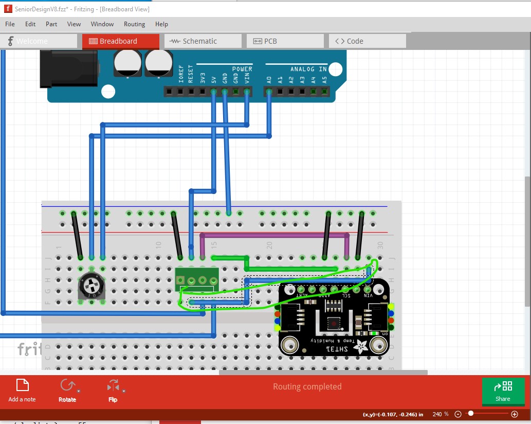
Here is what I have now…
SeniorDesignV8.fzz (34.2 KB)
This is what I am talking about the differences in SDA/SCL with the BB view vs PCB. Can you further clarify?
Also, I saw where you explained that connecting the pot to A0 is dangerous since Vin could be anywhere from 6 to 9V. The purpose of the pot there was to measure the voltage of the Arduino. Any suggestions on how to rewire this? The LCD screen will be connected via the JP3 pin as seen on the BB/PCB.
On the Uno there is an internal connection from A4/A5 to SCL/SDA so in pcb it routes to the closest point (A4 / A5 in this case.) On the Arduino WiFi Rev 2 (which is what you are actually using) SCL/SDA does not connect to A4/A5 as it does on the Uno. So changing to the Arduino WiFi Rev 2 Fritzing part will keep pcb from trying to use A4/A5 as SCL/SDA. You can also manually route the SCL / SDA traces to the proper pins on the UNO in pcb.
I just looked at the Adafruit site which says the sensor can be powered either by 3.3V or 5V so what you want to do is change the Vin on the sensor from 3.3V to 5V like this:
With the sensor running on 5V there is no need for level translation. In the original connection, the sensor is running at 3.3V but the I2C pins are being driven from the Arduino at 5V which can cause damage to the input pins on the sensor.
Assuming you want to measure the Vin voltage with the analog pin, you don’t need the pot but rather a fixed voltage divider. This circuit should do what you want.
two 1K resistors replace the pot. They will divide Vin in half (so 9V in will produce about 4.5V at the analog input pin.) then you need to scale the value of the analog input value by multiplying it by a scale factor to change the measured value to volts to display. I think the analog input is 10bits which is 1024 steps so it should be somewhat close as is, but what may be easiest in this case is to change the pot to be about 250 ohms and put it in series with the top resistor like this:
here I replaced the top 1K resistor with an 820 ohm resistor and a 250 ohm pot in series with it. Adjusting the pot will change the voltage at the junction of the resistors, so with 9V as Vin you should be able to adjust the pot so that the analog input reads 900 (equating to 9V) which is easier than calculating the scale value you need.
Peter
Thank you for ALL this information Peter!
I did not realize that this may cause issues, which makes sense when you point it out…“With the sensor running on 5V there is no need for level translation. In the original connection, the sensor is running at 3.3V but the I2C pins are being driven from the Arduino at 5V which can cause damage to the input pins on the sensor”.
I will change my schematic with the new pinouts and voltage divider and then upload it here to have you review one last time. Hopefully, I will be close to finish 
What are your thoughts? The schematic and PCB were not wanting to AR when I did it.
SeniorDesignV8.fzz (28.3 KB)
Hey Peter,
Here is the latest version. Please let me know your thoughts 
SeniorDesignV10.fzz (39.4 KB)
How do I know if I need to make a layer copper? Also what trace width would you suggest?
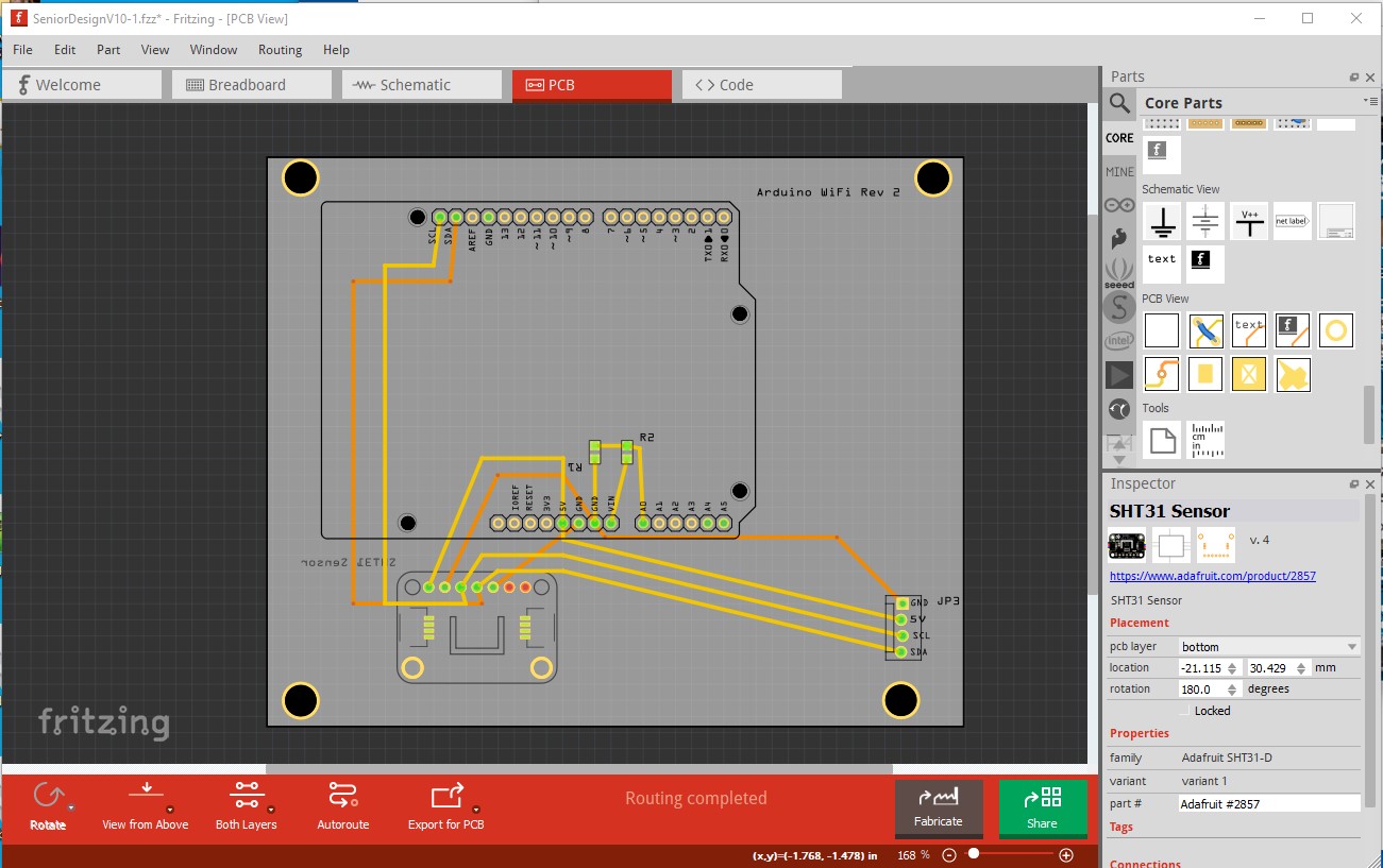
It looks fine except for a couple of issues. I deleted the trace to the smd pad on the sensor, it won’t connect (the sensor part shouldn’t have the smd pads in it very likely) and isn’t needed anyway. I added holes to the mounting holes on the arduino because by default they are not drilled (you are expected to drag holes in as I did if you want mounting holes.) and I assume you want mounting holes to fasten the arduino to the pcb.
and with the extra trace removed.
and the new schematic (I assume you autorouted schematic which usually does a lousy job of running traces!)
These changes are in this sketch:
SeniorDesignV10-improved.fzz (37.1 KB)
Have you considered that the Arduino is going to connect on the bottom of the board in the same place as the sensor? You will need to install male headers on the bottom of the board to connect in to the female headers on the Arduino which will mount below the board like this in order for the pins to match with the Arduino:
so you may need to move the sensor to the top of the board.
You can’t make a copper layer. There are only the top and bottom layers that Fritzing supports. You could make a single sided board but there is no advantage to it and the routing in pcb is more difficult. The default 24 mil trace width should do fine in this application, there is no high current here to need thicker traces.
Peter
Updated version with your suggested with trace. I am understanding your concern regarding the Arduino and how it would be on the bottom with the sensor since the Arduino currently has a female header, so then you would solder the male header to the PCB board and then insert into the the female header on the Arduino, is that correct?
I want the sensor on the top of the board (or vice versa with the Arduino on top and sensor on bottom).
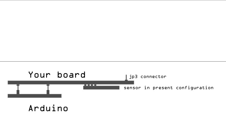
I have attached a sideview of the design with the sensor on bottom then the base of the enclosure is exposed to the environment, while the Arduino is still protected.
SeniorDesignV11.fzz (37.7 KB)
Also, can I ask what software you used to make the above side view? It looks great!
Given what I see in the thread, you could probably turn your board into a shield for the Arduino. Make the PCB the size of the Arduino (or just big enough to hold the headers). With or without ‘mounting hardware’. Mount your sensor and external header/connector on the top of that. Unless you need more separation from the Arduino electronics.
How would you suggest mounting the Arduino to the enclosure to ensure it does not move around in the enclosure? Currently, there are places to mount the PCB in the enclosure, thus, the drill holes on the outer edge of the PCB. I am ALL ears so if you have a better solution, please share. I don`t mind mounting everything on top and using the PCB like a shield, just curious on how I might then mount the Arduino to the enclosure.
I did not see anything previous in the thread about a specific enclosure. I was writing my post the same time as you were doing the one with the side view. If that is a project constraint, then the large PCB may be the best option. The Ardunio board has mounting holes as an alternative, but that would be a different footprint. About half the size, not counting the battery pack.