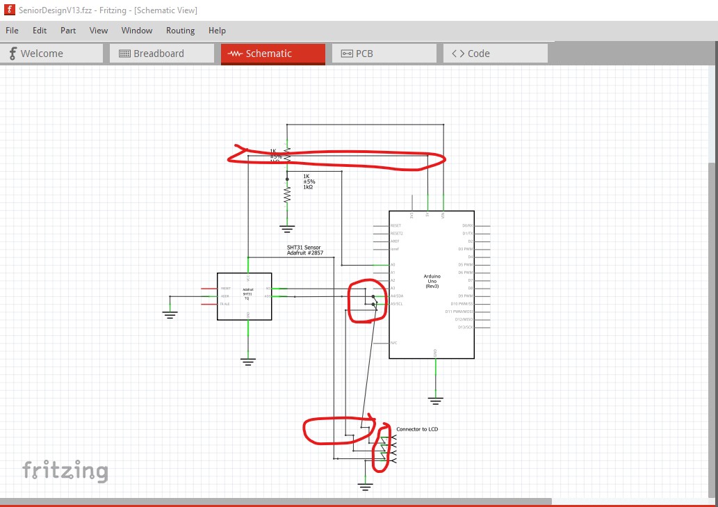
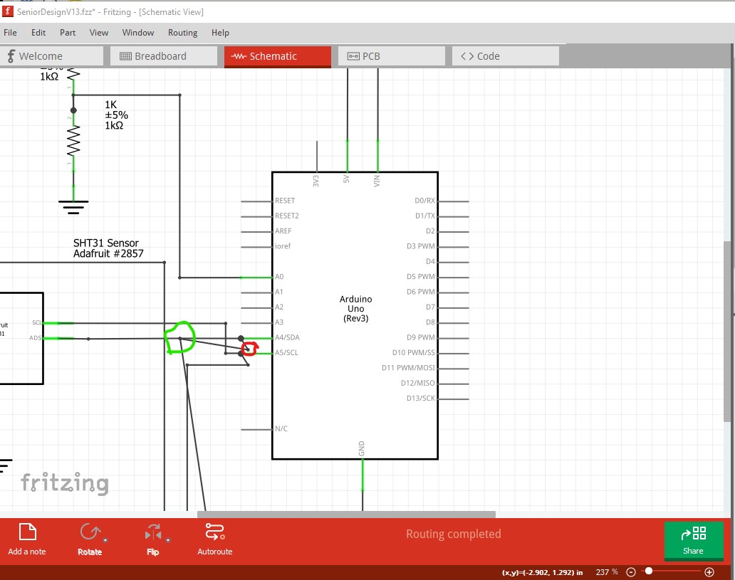
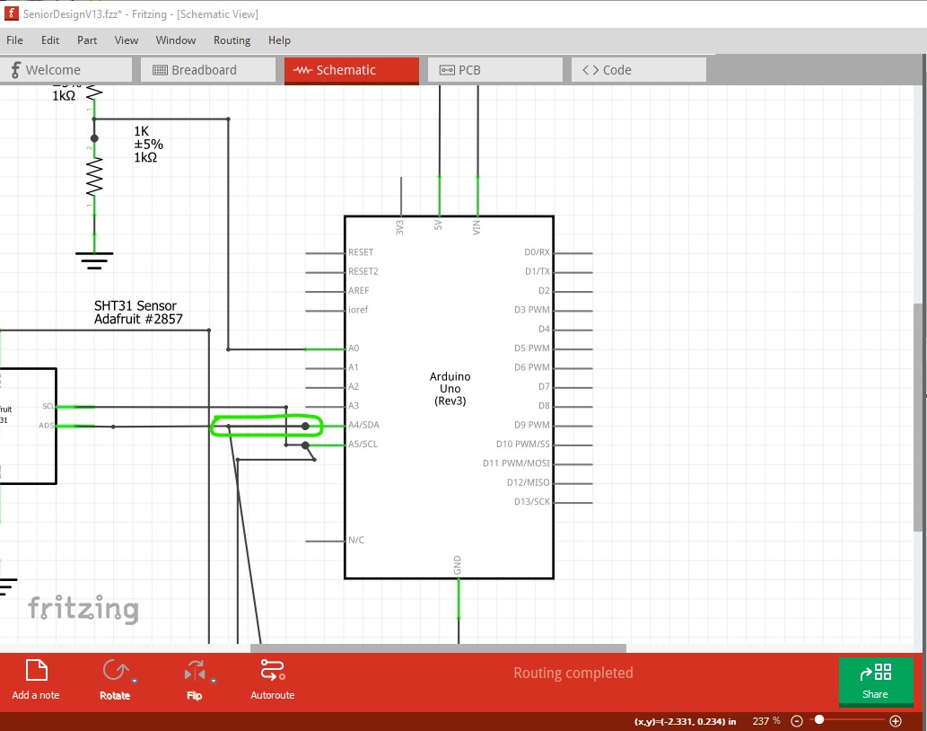
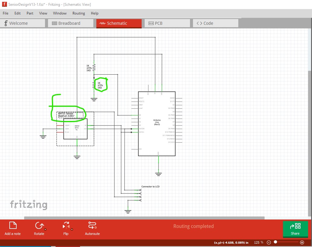
On the schematic view, the routing makes it look like the 5V line from Arduino to the LCD connector is ALSO connected to A0. The wires are right on top of each other, and the bend corner looks almost like a connection (join) point. Same for the wire from A4 to the LCD connector. It looks like it is also connected to A5. They are not connected, it just looks like it.
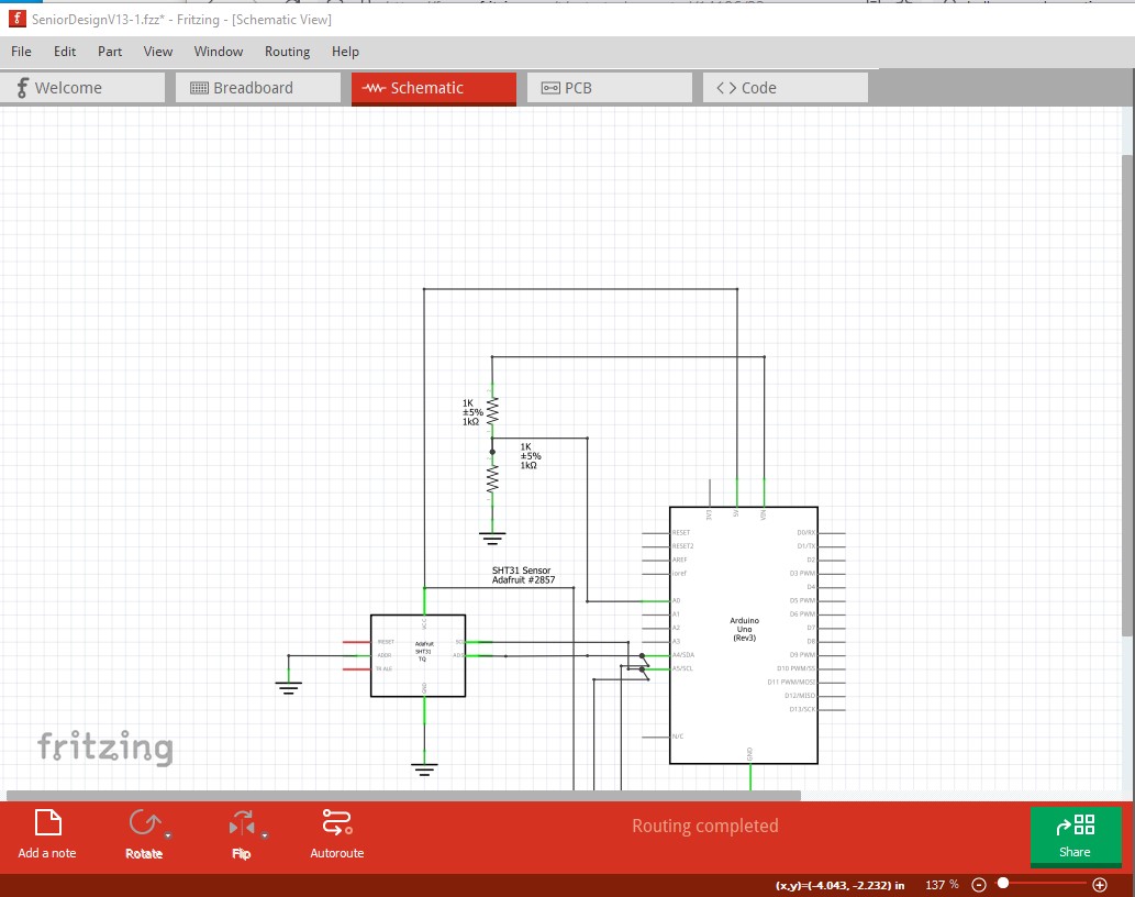
If the resistors are just a voltage divider for monitoring the input source voltage, 1K is lower than needed (drawing more current). Increasing them to 10, or even 100K should be better.
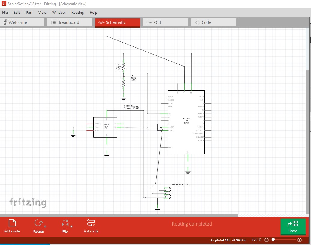
The resisters both have a label of ‘1K’ (set in Inspector). Using ‘R1’ and ‘R2’ would be more common. Which properties of the parts are to be displayed in each view is controllable from the label. Right click the label (not the part), and (un)select options under “Display Values”.
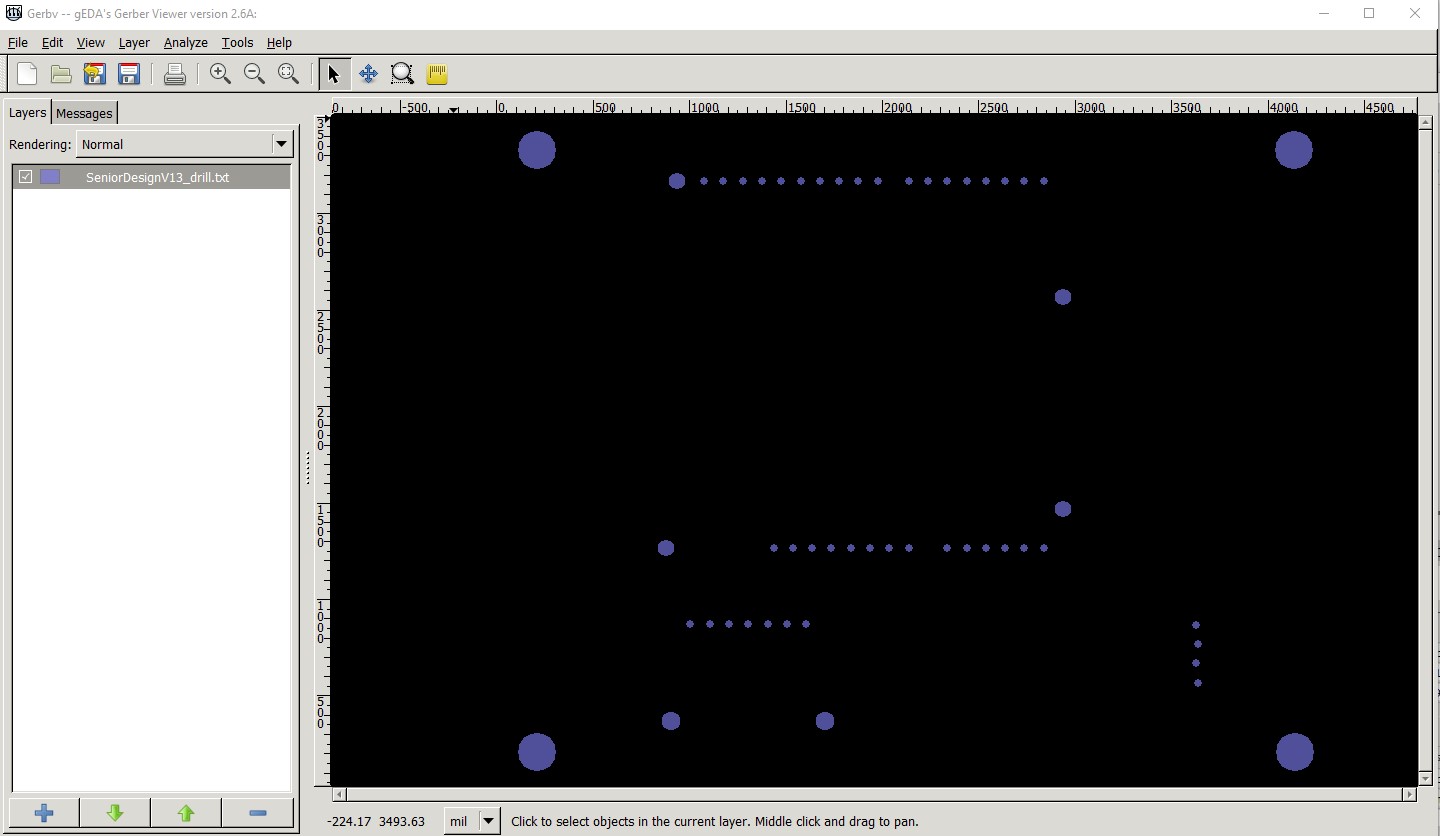
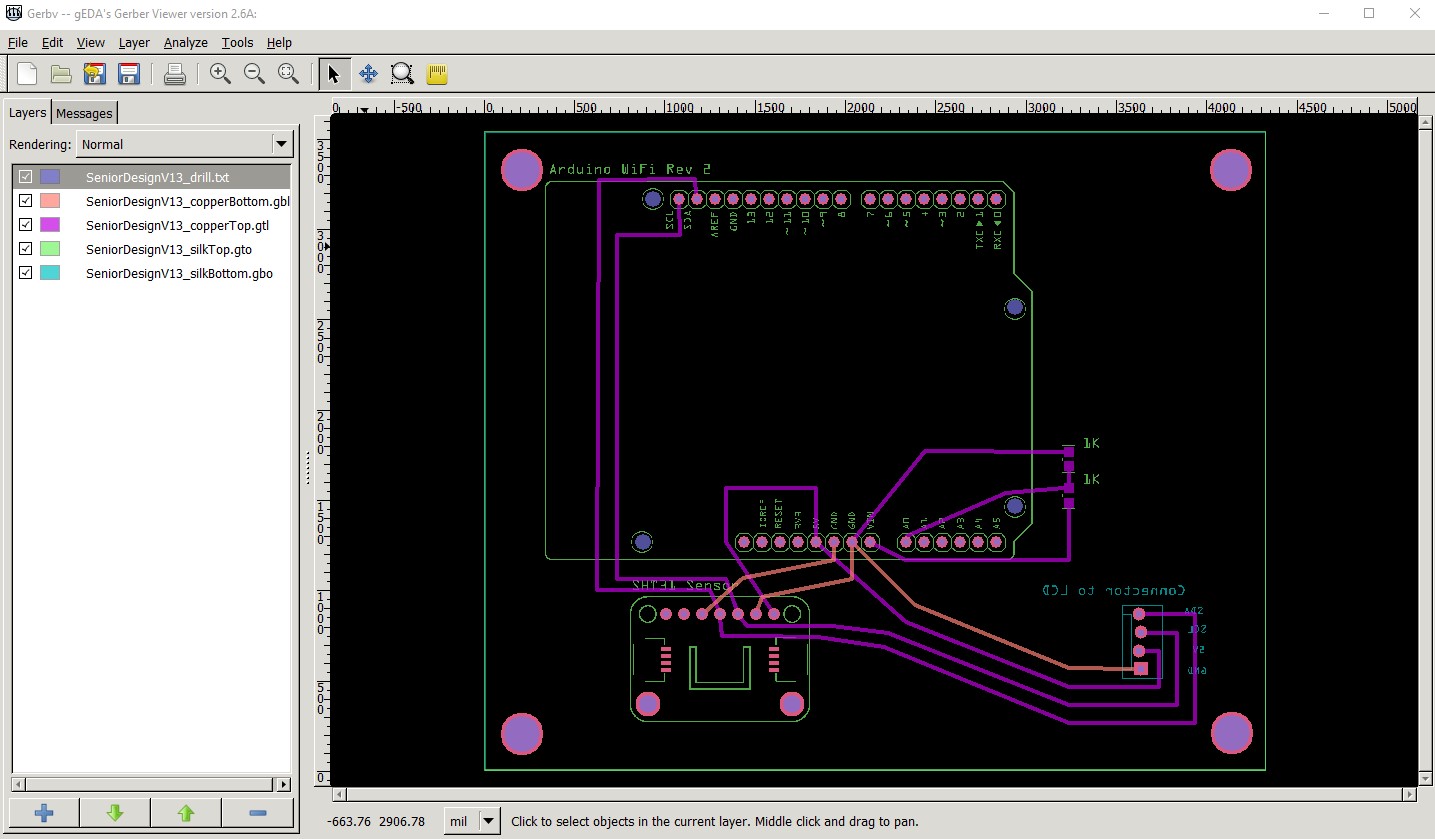
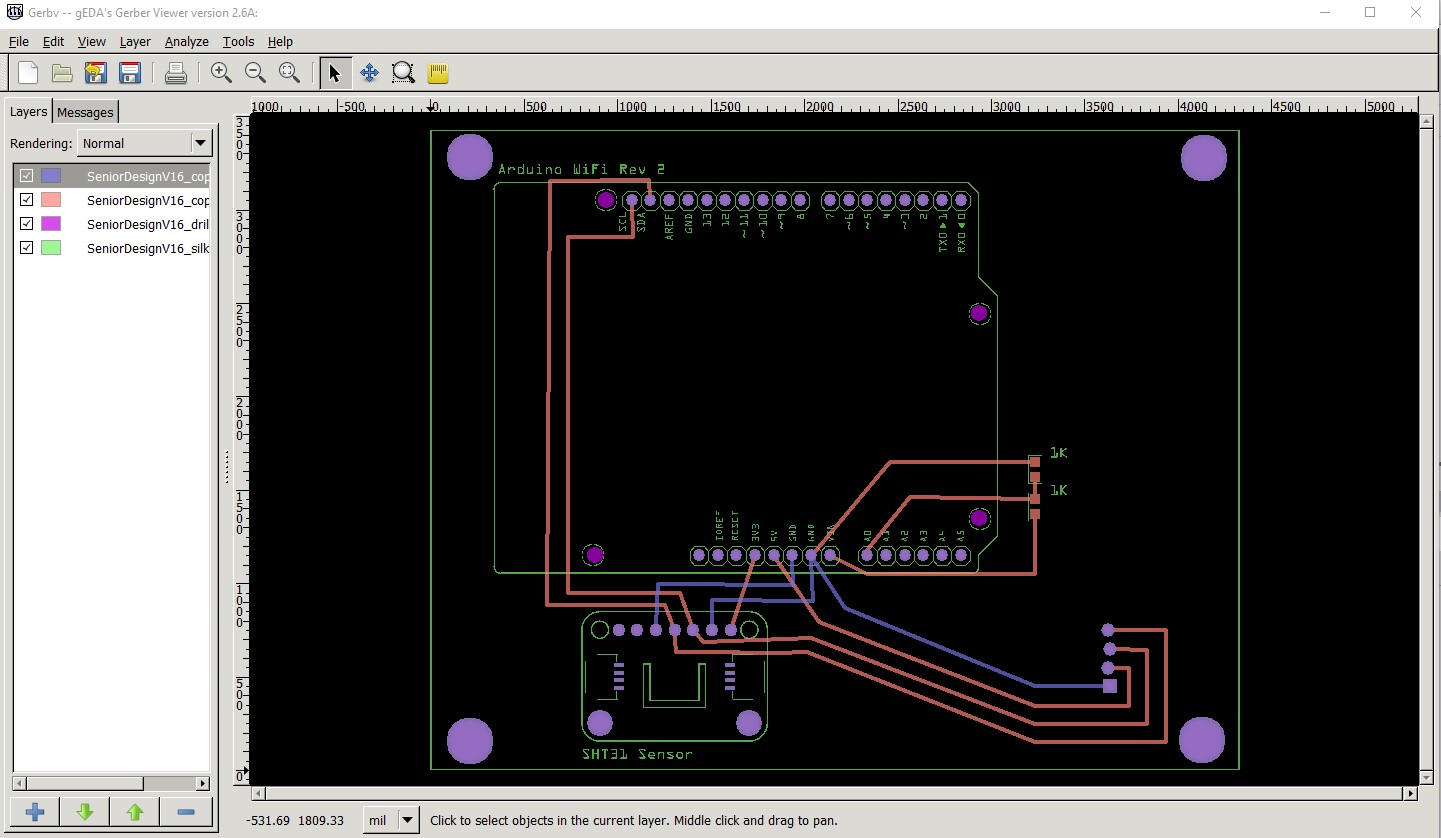
On PCB, instead of running a trace from each of sensor pins to different GND pins on the Arduino, you could run a trace from one sensor pin to the other, then a single trace from one of those pins to a GND on the Arduino.
I do not know what the physical constraints are for your project, but rotating the LCD connector 180° would make the routing of the traces cleaner. No need to go ‘around’ the connector.
There does not seem to be any need to have the SCL trace from the Arduino to the sensor pin route around the bottom Arduino mounting hole. Straight through the middle works fine. Switching the SDA trace to the bottom layer means it can run directly across as well.
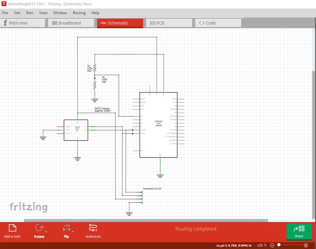
On schematic view, you can use “Power” symbol parts for the various power bus lines. That simplifies the routing quite a bit. More so, if there were more parts.
Since the Ardunio does not mount ‘flat’ to the PCB, the SMD resistors could be placed under the Arduino. Shortening the traces considerably. Adjusting the routing of the traces to the connector allows (what I did here) the resistor traces to be shortened, while keeping just outside of the Arduino pins.
Are those SMD pads on the sensor “really” flush with the PCB? Design rules check complains if a trace from the sensor pins runs across them. I “expect” that those are on the sensor board, but do not connect to the pcb, so a trace across them (on the PCB) would be just fine.
This version of the part file has those, and a few other ‘personal preference’ adjustments. I did not look at the gerber output for either the original or my modified version. This was just some hints for alternate ways of doing the same thing, and trying to reduce confusion when looking at the drawings.
SensorDesignV16.fzz (38.3 KB)