mini560-buck-dc-dc-converter.fzpz (14.0 KB)
This is the Fritzing part for the Mini 560 Buck DC-DC converter which can be found at Mini560/Mini560 PRO 5A DC-DC Step-Down Stabilisiertes Spannungsversorgungsmodul 6-30V bis 3,3V 5V 9V 12V - AliExpress 502
Welcome aboard! Good job! The part appears to be pretty much perfect. For some reason the AI looks to have blocked the post, I will inquire as to what went wrong as I don’t see anything that should cause a block, but the AI blocking is fairly new (if that is what did the block, which I am not sure of.)
Peter
Thanks for the feedback, I am new here and am looking forward to contribute more!
The shop seems to use copy protection (splitting and water marking images), so it doesn’t seem to be intended for sharing here in the forum.
Do you have manufacturer links instead of links to a shop?
About the part:
It has a “stamp hole design” with a flat bottom (no parts mounted), and can be directly soldered on top of a PCB. This would only work if the dimensions are exactly that of the part.
It would be really nice if the footprint in the PCB could be used for this, especially since the part is designed for it.
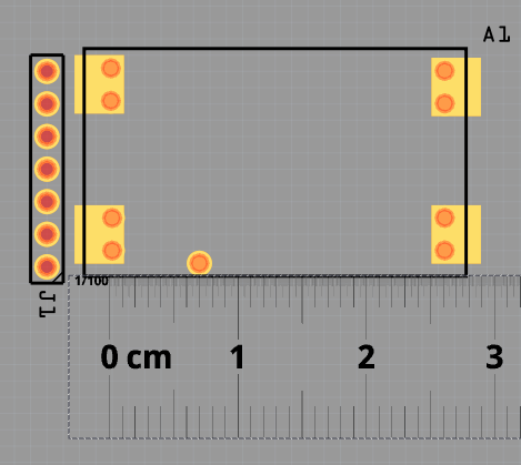
The distance between the connections on the shop website says 29mm, but in the part, the distance is only ~26mm . So soldering the part on top of a PCB would not fit:
You are off to a good start! Your first part (I expect the AI blocked the rest before I saw them, that has now apparently been fixed so it shouldn’t block them in future) was close to prefect making me think you were using FritzingCheckPart.py which has this to say about your part:
$FritzingCheckPartw.py part.mini560-buck-dc-dc-converter.fzp
**** Starting to process file Startup, no file yet
**** Starting to process file part.mini560-buck-dc-dc-converter.fzp
**** Starting to process file svg.breadboard.mini560-buck-dc-dc-converter_breadboard.svg.bak
**** Starting to process file svg.schematic.mini560-buck-dc-dc-converter_schematic.svg.bak
**** Starting to process file svg.pcb.mini560-buck-dc-dc-converter_pcb.svg.bak
File
‘part.mini560-buck-dc-dc-converter.fzp.bak’
This is a through hole part as both copper0 and copper1 views are present.
If you wanted a smd part remove the copper0 definition from line 54
Modified 7: File
‘svg.breadboard.mini560-buck-dc-dc-converter_breadboard.svg.bak’
At line 2952
A Tspan was removed.
Check the output svg is correctly formatted after the change.
Modified 4: File
‘svg.schematic.mini560-buck-dc-dc-converter_schematic.svg.bak’
At line 33
ReferenceFile
‘mini560-step-down-module_1_schematic.svg’
doesn’t match input file
‘mini560-buck-dc-dc-converter_schematic.svg’
Corrected
Modified 4: File
‘svg.pcb.mini560-buck-dc-dc-converter_pcb.svg.bak’
At line 31
ReferenceFile
‘mini560-step-down-module_1_pcb.svg’
doesn’t match input file
‘mini560-buck-dc-dc-converter_pcb.svg’
Corrected
Error 94: File
‘svg.breadboard.mini560-buck-dc-dc-converter_breadboard.svg.bak’
The svg has been modified (details in the Modified section).
Examine the svg with a svg editor to make sure it is correctly formatted.
The tspan removal error (which is easy for me to fix by removing the xml:space=”preserve” attribute which is disturbing lxml) indicated you had done something to remove px from the font-sizes (which Inkscape which you appear to be using usually adds.) Your Arducam Mega 3MP SPI OV5642 part has a lot more errors that I will detail in a while. Since it looks like you may not has seen it, this tutorial will give you information on fixing the issues (there are 14 or 15 chained parts to the tutorial following this one":
I will also have a look at the points @KjellM raised and detail how to make a part that will fix them (which will likely mean adding a SMD part to allow the board to be soldered down, at this point I haven’t looked closely at it yet.) More to come.
Peter
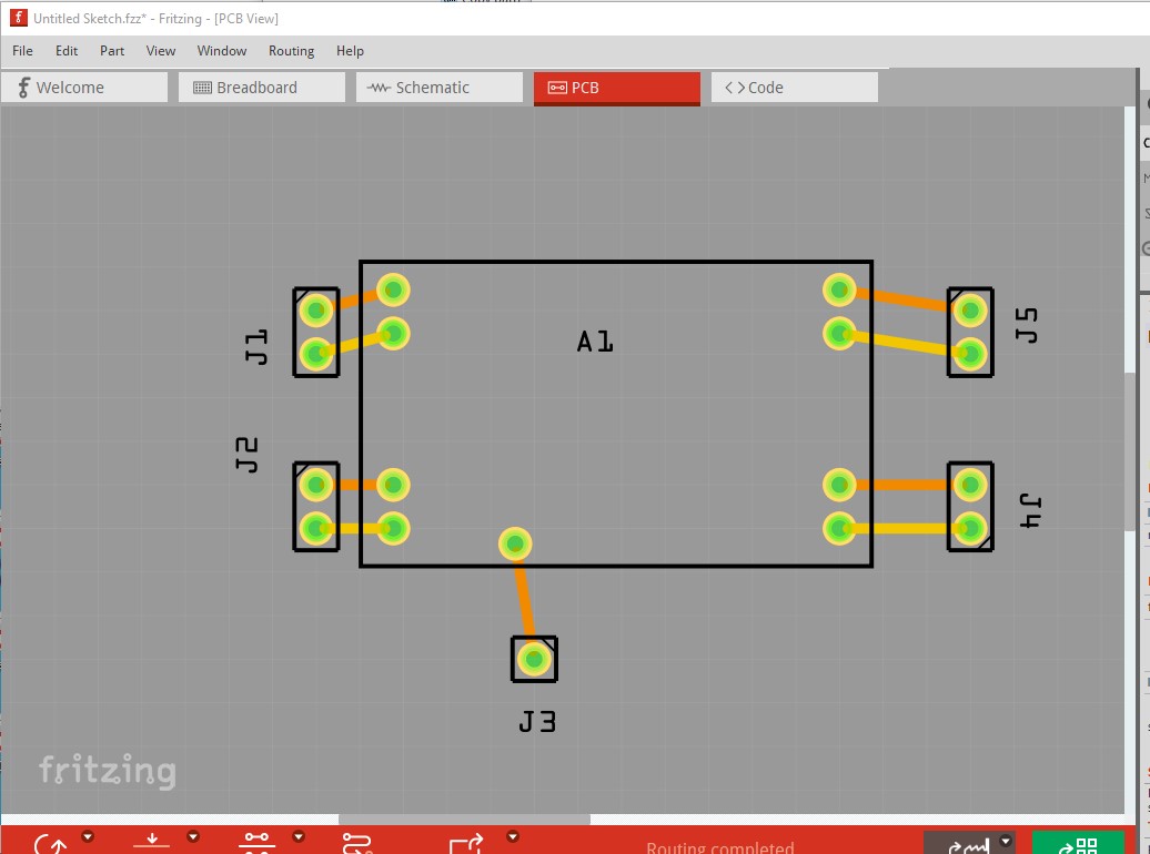
It appears @KjellM is correct, your pcb layout looks wrong. I have made a corrected version (and added a SMD part as well) but because it is from a jpeg image it may still be incorrect. The best answer is to print out the pcb footprint at 1:1 scale (the default) preferably on transparent overhead film and compare it to a real part to make sure the holes line up. Here with Inkscape I imported via file→import a jpeg image of the pcb then moved the square pads clear of the circles and scaled the image down to match the size of the silk screen outline (which matches the dimensions in the jpeg) that should give a pretty good (but not perfect) position for the pads. I also increased the radius of all the pads using xml editor (which increases the size if the circle while leaving it centered in its current position which is important here!) and set the fill value from white (#ffffff) to none so the image will show through in the hole in the center of the circle to aid placement.
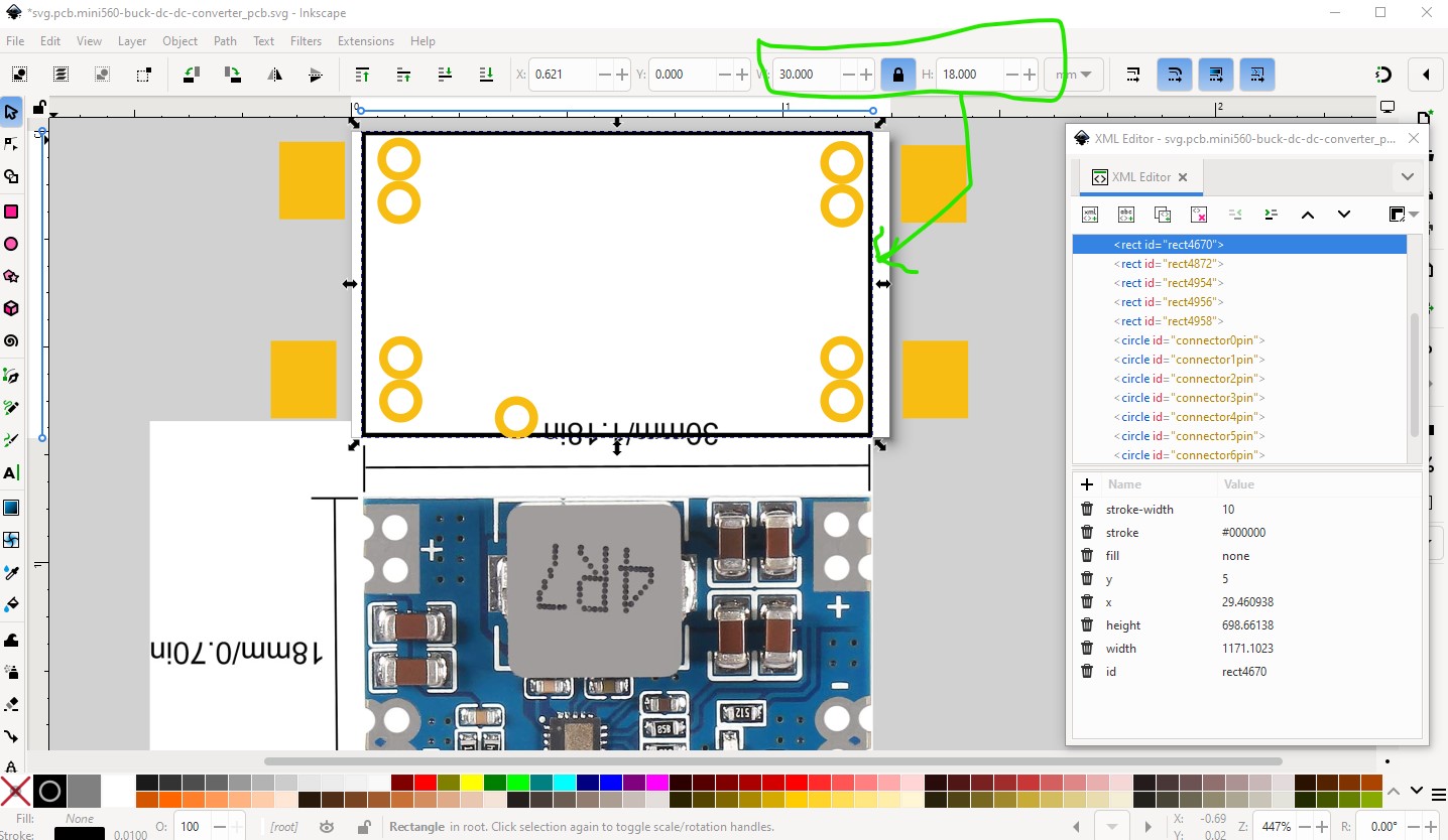
With the image moved to exactly (as far as I can see) cover the silkscreen outline we see that the pads are slightly misaligned (circled in red here.)
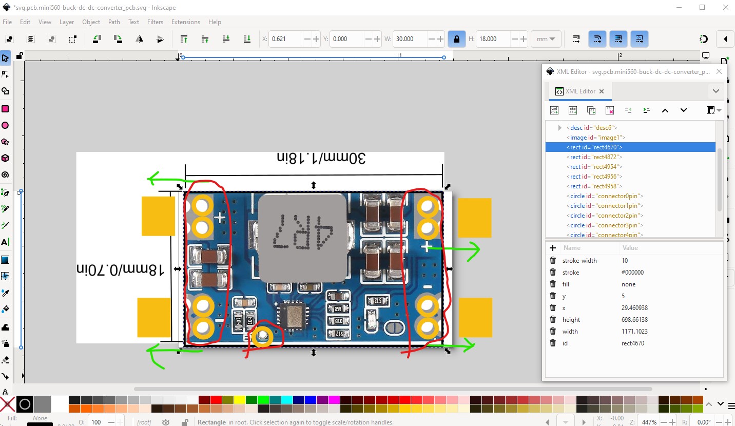
Since the pads are correctly on 0.1in boundaries I selected the pads in pairs except of the enable pad which is a single) then moved them so the holes were as close as I could get them to the center of the circle in the jpef image via the Inkscape toolbar.
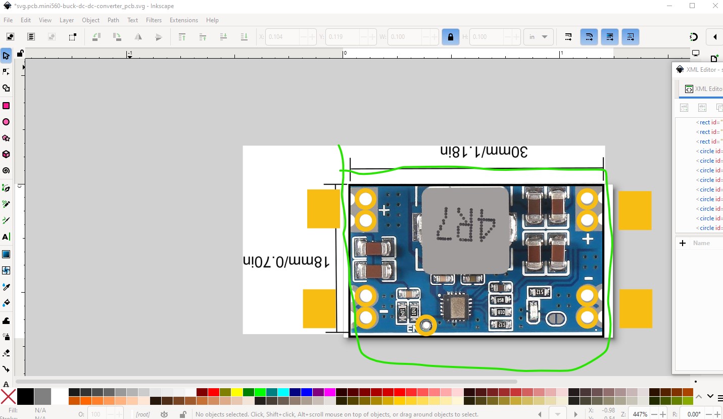
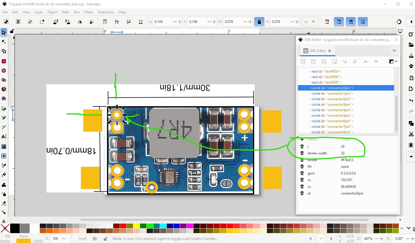
This I think should be a more accurate (but as noted possibly not accurate enough until verified against a real physical part) to position the pads more correctly. For the THT part I choose to delete the copper pads leaving only the holes (we will add the pads to the SMD version of the part later.) Now the pads are over sized (a radius of 40, instead of the 29 for a 0.1in header that they should be) so now go through and change the radius back to 29 in xml editor which again will reduce the size of the circle without moving it in x and y (which a normal move will do.)
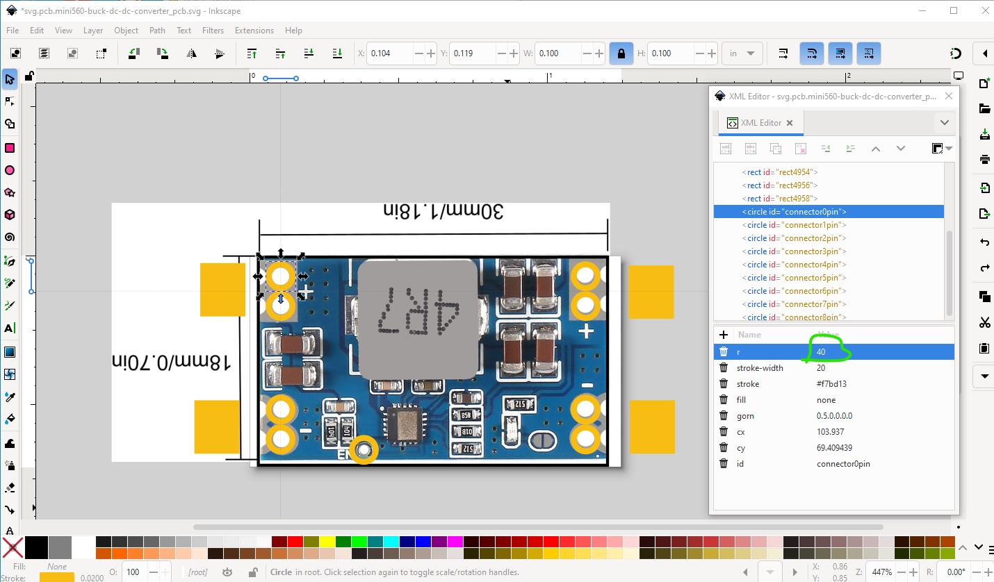
Here is the first pad done where we can see it did not move in x or y when reduced in size (the advantage of changing the radius in xml editor.)
When completed the final pcb svg looks like this
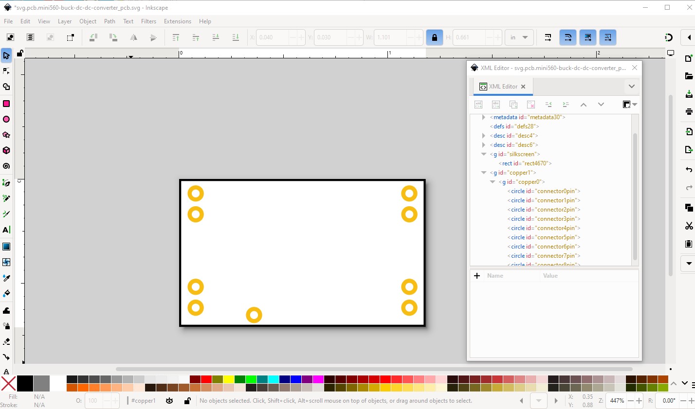
which is contained in this part (the moduleId of this part is the same as the current part so if you have the current part loaded, you will need to delete the current part from your mine parts bin, then shutdown Fritzing answering yes to the save parts prompt and yes to the save parts bin prompt but no to save sketch in order to really delete the part. Upon restarting Fritzing you should be able load the new part with the new pcb and print out the footprint at 1:! and compare it to a real part.
If the pads don’t line up with a real part, then you need to move them in the pcb svg until they do. Now to make an SMD version of this part. Breadboard and schematic will be identical for both parts (although the file names need to change.) The fzp file and the pcb svg need substantial changes though. First import and scale the same jpeg I used above
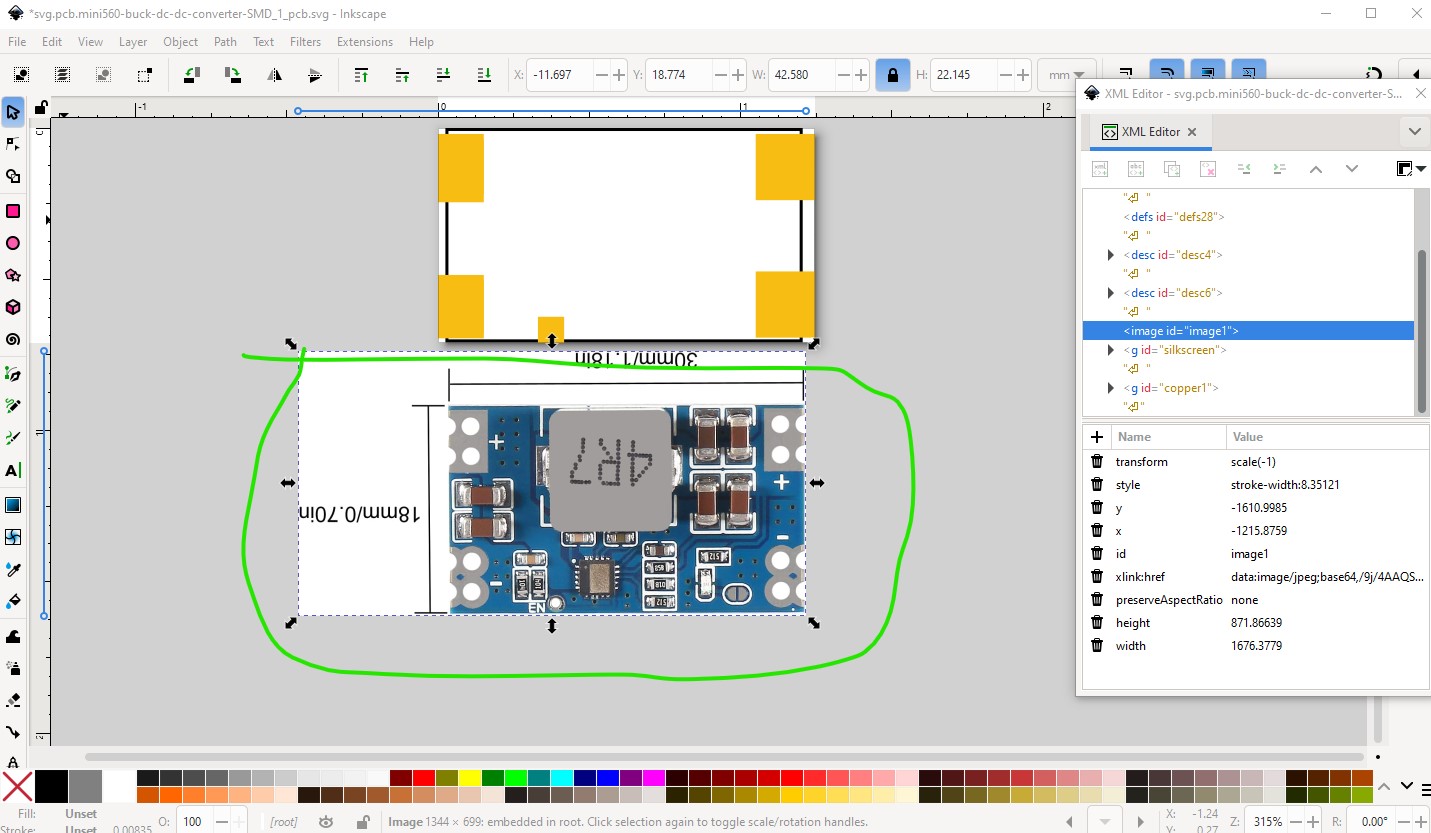
Then overlay it on the silkscreen outline
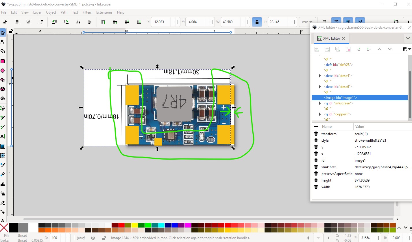
Then expand the existing rectangular pads to cover the pad on the board plus a bit of space beyond the board to provide a way to position the board before soldering. Note that the double pads need to exist to provide connectors, here I overlaid them which will put them on top of each other like this (this is connector0, with connector1 overlaid on it)
like this.
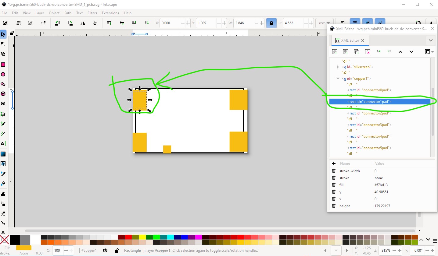
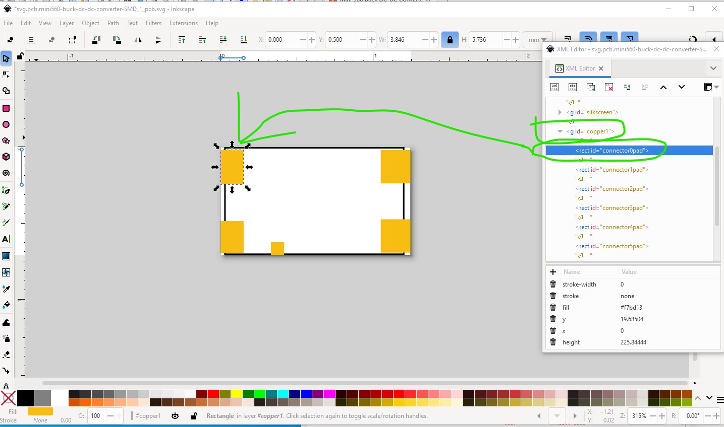
Then we need to modify the .fzp file, in this case I just edited the .fzp file with a text editor and made the necessary changes. That is the file names for the new svgs (which need to be unique) and removing the copper0 group from the pcbview definition to change this:
        <pcbView>
          <p svgId="connector0pin" layer="copper0"/>
          <p svgId="connector0pin" layer="copper1"/>
        </pcbView>
to this
        <pcbView>
          <p svgId="connector0pad" layer="copper1"/>
        </pcbView>
just delete the copper0 definition to change the board from through hole to SMD. Now for each of the connectors, change
        <pcbView>
          <p svgId="connector0pin" layer="copper0"/>
          <p svgId="connector0pin" layer="copper1"/>
        </pcbView>
to
        <pcbView>
          <p svgId="connector0pad" layer="copper1"/>
        </pcbView>
which deleted the copper0 definition and changed the connector0pin to connector0pad. Pin would work fine (as long as the svg matched it) but Fritzing convention is to use pad for SMD pads. Doing all this results in this part which implements the same part in a SMD component. I could have added the copper pads to the existing through hole part which would have worked fine, but the pads would appear on both the bottom and the top of the board. With the SMD part definition it is possible (but possibly not wise, because of magnetic interference between the 2 parts) to place on part on the top of the board and another part on the bottom of the board in the same position as the one on the top. With a through hole part that is not possible because the pads are on both sides of the board. (although that can be gotten around with enough work, it is very messy!) Here is the SMD version of the part:
mini560-buck-dc-dc-converter-SMD.fzpz (13.5 KB)
Hope this helps, as always if you have questions please post and I will try and answer them.
Peter