I wanted to build a roughly triangular area copper-filled, tied to net +5V.
Here is a portion of the schematic:
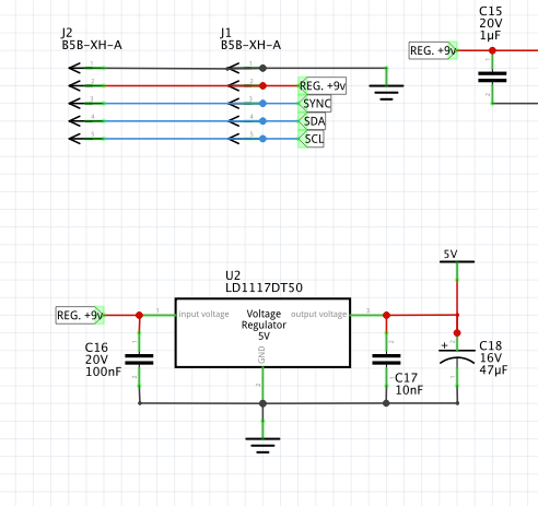
I wanted to tie the +5 on U2 (Vout), C17, and C18 on the YELLOW side together with a fairly large pad, and connect this to the RGB LEDs with a +5V bus on the ORANGE side of the board.
I accomplished this with 6 vias. Here is the PCB view, from the TOP:
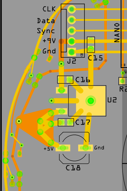
First I added the 5 intermediate Vias. Then I connected U2, C17 and C18 (all on the YELLOW side) with 48mil traces to 3 Vias. And interconnected those also to two other Vias.
Then I drew this triangular fill area, by connecting the 6 Vias to each other with 100mill traces.
The result is pretty good! This might be overkill, however, since all the failures in my previous board layout were power and voltage-drop related, a little overkill is good.
Next, I will ground-fill the top (YELLOW) side; and copper-fill the rest of the bottom (ORANGE) side.
-allan schwartz