I hate to come on here again asking for help with another part, but I attempted to create one and it just isn’t working. I will link the part if anyone notices problems, but also know that I didn’t really do anything for the breadboard side of the component because I won’t be using the breadboard. Any help or tips would be greatly appreciated.
You need to upload the .fzpz file for the part. The fzp is only the defining xml, it doesn’t have the associated svg files with it (the fzpz file contains them all.)
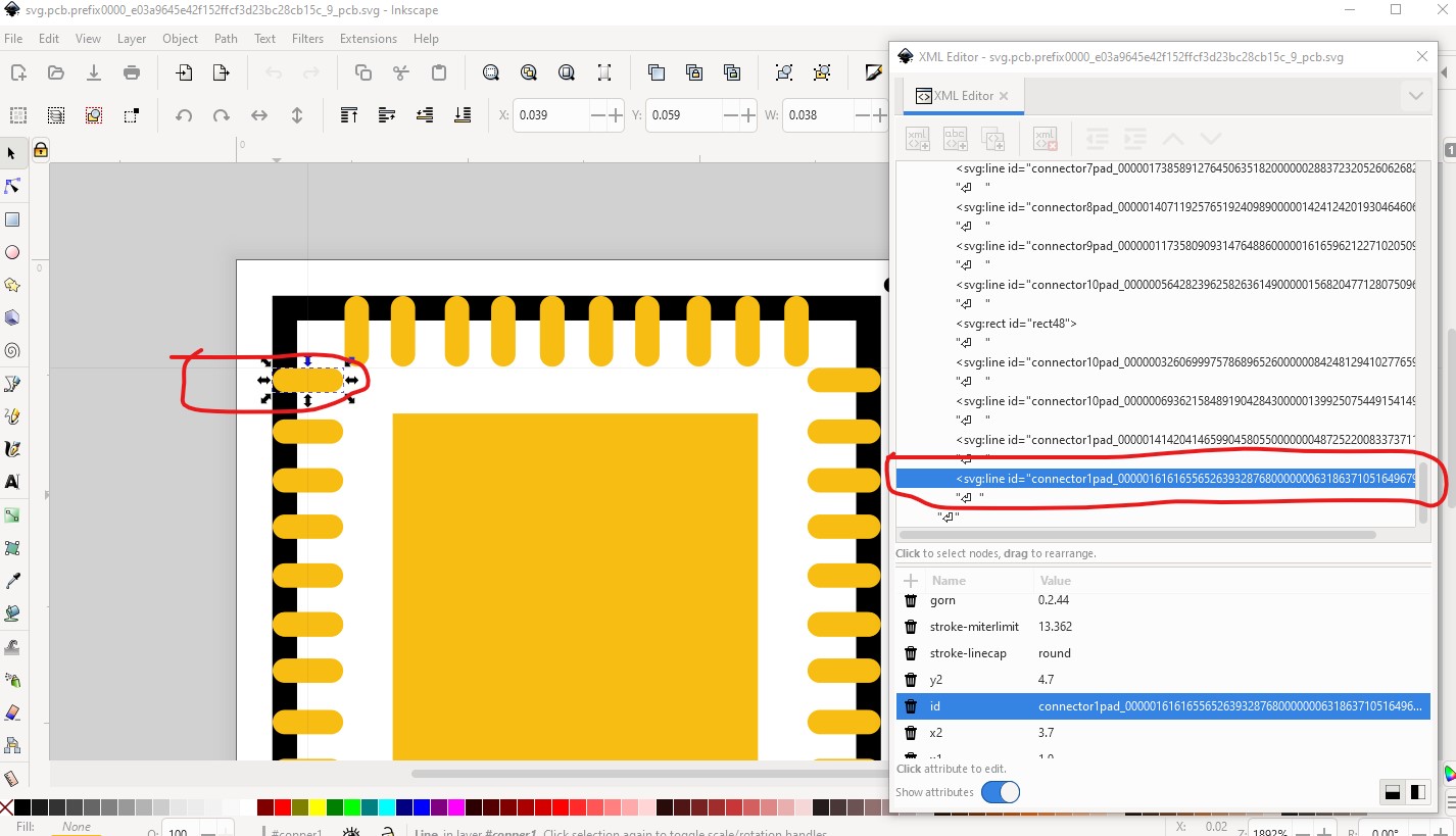
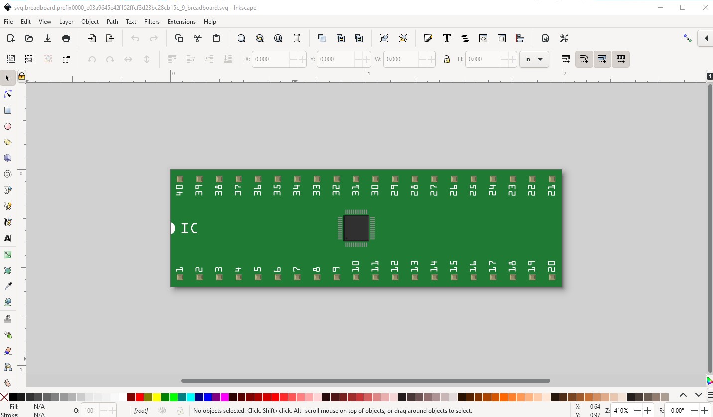
note the copper1 connector is connector0pin, however in the pcb svg it is known as
“connector1pad_00000161616556526393287680000000631863710516496791_” which doesn’t match the label in the fzp file and thus the connector isn’t defined (it should be connector0pad). This is the pcb svg displayed in Inkscape:
The fix is fairly easy, just correct the pin labels in the svg. After that it looks like the footprint needs some adjustment. I grabbed the jpg image of the footprint from this site:
and overlaid it on the pcb svg in Inkscape like this:
As we see, the pads need to move out a bit to be correct. So do that as well, and pin 1 (on the top left) should be a rectangle as well as the dot (which is currently in the wrong place) for pin 1.
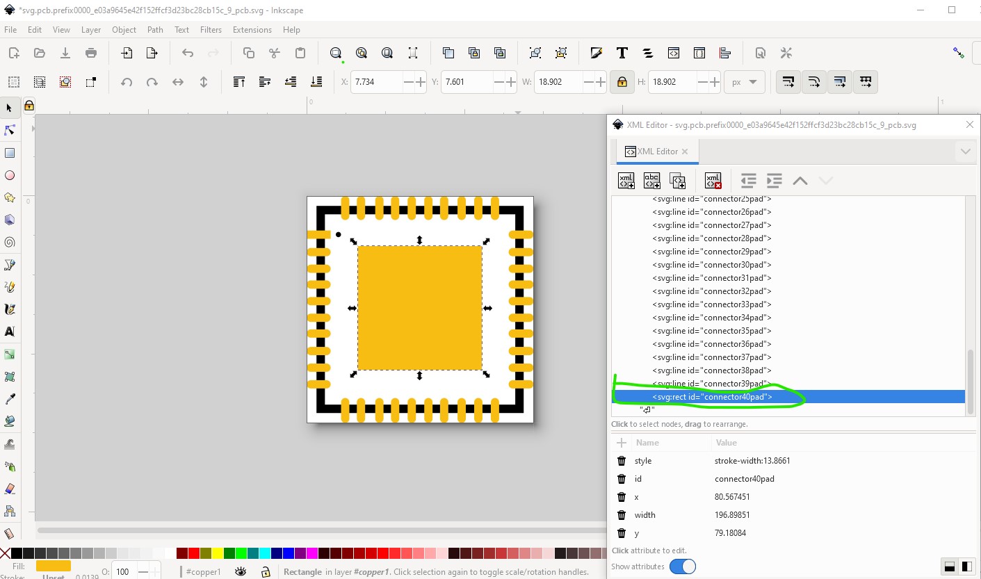
in addition I gave the thermal pad a connector number (connector40pad) in case you need to ground the thermal pad. I haven’t added it to the fzp file though so it won’t show up as a connector. There is now enough clearance between the pads to run a trace to the thermal pad if required. Then I replaced the breadboard svg with this one (which is how SMD parts are typically displayed in breadboard)
I replaced the schematic svg with one generated by Randy’s Inkscape extension (most very thing I did here is available in this tutorial set if you have not seen it:
)
then fixed up the fzp file to make sure the pin numbers match correctly. That mostly involved changing the type from pad to male (which is what type should usually be!) and then changing the pin to pad for the pcb connector definition.
Doing all that results in this part which should do what you want. Note before ordering boards it is advisable to print the pcb footprint out at 1:1 scale and compare it to a real part to make sure it is correct.