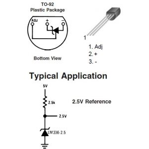
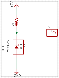
I am trying to generate by myself a new component, but it doesn’t work correctly… What am I doing wrong?

LM336 BZ-2.5.fzpz (6.9 KB)

I am trying to generate by myself a new component, but it doesn’t work correctly… What am I doing wrong?

LM336 BZ-2.5.fzpz (6.9 KB)

To some extent you have been fooled by bad practice in reusing svg files in core parts. Breadboard appears correct
the header labels match the correct pin numbers.
schematic is wrong in several ways
the terminalIds are incorrect (which is what is causing the wires to connect to the center of the pin rather than the end) and connector0 is connected to the wrong pin in schematic. Pcb has the order of the pins backwards connector0 and connector2 need to be swapped.
This is caused by the core part doing tricks to reuse svgs which makes making changes difficult unless you understand what was done. The errors are in the fzp file
    <connector id="connector0" name="ADJ" type="male">
      <description>Adjust</description>
      <views>
        <breadboardView>
          <p layer="breadboard" legId="connector0leg" svgId="connector0pin"/>
        </breadboardView>
        <schematicView>
          <p layer="schematic" svgId="connector0pin" terminalId="connector0terminal"/>
        </schematicView>
        <pcbView>
          <p layer="copper0" svgId="connector2pin"/>
          <p layer="copper1" svgId="connector2pin"/>
        </pcbView>
      </views>
    </connector>
should change to
    <connector id="connector0" name="ADJ" type="male">
      <description>Adjust</description>
      <views>
        <breadboardView>
          <p layer="breadboard" legId="connector0leg" svgId="connector0pin"/>
        </breadboardView>
        <schematicView>
          <p layer="schematic" svgId="connector0pin" terminalId="connector0terminal"/>
        </schematicView>
        <pcbView>
          <p layer="copper0" svgId="connector0pin"/>
          <p layer="copper1" svgId="connector0pin"/>
        </pcbView>
      </views>
    </connector>
connector1 is correct as it stands
    <connector id="connector1" name="+V" type="male">
      <description>Voltage</description>
      <views>
        <breadboardView>
          <p layer="breadboard" legId="connector1leg" svgId="connector1pin"/>
        </breadboardView>
        <schematicView>
          <p layer="schematic" svgId="connector1pin" terminalId="connector1terminal"/>
        </schematicView>
        <pcbView>
          <p layer="copper0" svgId="connector1pin"/>
          <p layer="copper1" svgId="connector1pin"/>
        </pcbView>
      </views>
    </connector>
connector2 needs to change from
    <connector id="connector2" name="GND" type="male">
      <description>Ground</description>
      <views>
        <breadboardView>
          <p layer="breadboard" legId="connector2leg" svgId="connector2pin"/>
        </breadboardView>
        <schematicView>
          <p layer="schematic" svgId="connector2pin" terminalId="connector2terminal"/>
        </schematicView>
        <pcbView>
          <p layer="copper0" svgId="connector0pin"/>
          <p layer="copper1" svgId="connector0pin"/>
        </pcbView>
      </views>
    </connector>
to
    <connector id="connector2" name="GND" type="male">
      <description>Ground</description>
      <views>
        <breadboardView>
          <p layer="breadboard" legId="connector2leg" svgId="connector2pin"/>
        </breadboardView>
        <schematicView>
          <p layer="schematic" svgId="connector2pin" terminalId="connector2terminal"/>
        </schematicView>
        <pcbView>
          <p layer="copper0" svgId="connector2pin"/>
          <p layer="copper1" svgId="connector2pin"/>
        </pcbView>
      </views>
    </connector>
to associate the correct pins to the correct connector definitions in the fzp file. Then the schematic svg needs some corrections. The adj pin needs to be connector0pin (and have connector0terminal added!)
This pin needs to change to connector1pin (and connector1terminal added) to be correct.
this pin is correct but needs connector2terminal added.
Then the font sizes need adjusting to make the text a reasonable size. All of that (the instructions for which can be found here)
result in this part
LM336 BZ-2.5-fixed.fzpz (6.5 KB)
(you will need to delete the current part from your mine parts bin, then restart Frtizing to really remove it before you can load the new version) which looks like this
Peter
Thank you Peter for the info and the explanation. I am learning a lot. ![]()
Part creation is complex and tends to bite without warning!
Peter