(original post missing)
Dec 2021, @vanepp wrote
Welcome aboard! Your part has a few issues. The most serious is that the pcb layout isn’t SMD and the part is. Here is an improved version with the following changes:
breadboard:
Convert to an adapter board that converts from SMD to .1in DIP spacing which is typically how SMD parts are represented in breadboard in Fritzing.
schematic
replace completely with one made with the Inkscape Fritzing extension which produces a schematic which meets the graphics standard (this is strictly cosmetic, the original would have worked, just doesn’t meet the standards.)
pcb
replace the footprint with a SMD version (and modify the .fzp file to remove the copper0 layer from pcb to make an SMD part!) This part has a new moduleId and thus will load along side your original part for comparison.
LM2731-improved.fzpz (4.6 KB)
Peter
Thanks Peter! I was aware about the SOT23 issues, and thought those were corrected already, but the rest was new ![]()
Edit: @vanepp , I am struggling to find a guide on the correct layers (and their purpose, so what should be placed where) for SMD parts, do you happen to have one?
New try for another part: TC1108 3.3V Voltage Regulator by Microchip, Microchip TC1108-3.3VDBTR
TC1108.fzpz (6.7 KB)
The part file format document available here has the layouts
The difference between a through hole and a SMD part is that that SMD part only has the copper1 layer in pcb view where a through hole part has copper0 as a child group of copper1 and the copper appears on both sides of the board. An older format that had separate copper0 and copper1 layers (but for through hole the pads had to appear on both copper layers) is still supported and is sometimes useful for doing odd things. This tutorial series may help as well, as it describes how I make parts by editing the files themselves.
Part creation howto part 1 breadboard and pcb
As well you may want to change to the parts-submit forum category as posts here in About the parts submit category are not show as new posts in the forum (I expect there is something special about this particular topic) so most people won’t see the posts. I only came across it because the tool bar said there were unread posts even when there didn’t appear to be any. Clicking on it took me here.
Peter
Schematic is incorrect. Connector1 and connector2 are reversed which makes the schematic connection wrong (possibly in the original part you cloned from.)
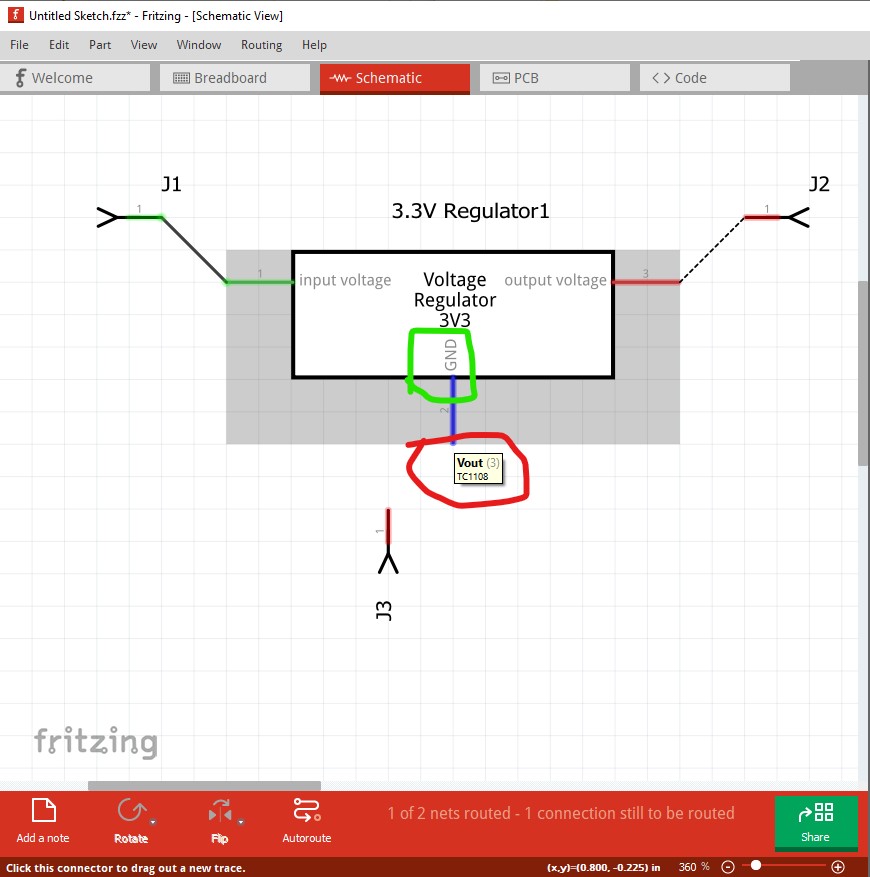
Here pin 2 is labeled as ground which is correct, but hovering on the pin indicates that it is Vout which isn’t correct. That is because the .fzp file has the schematic pins reversed (FrtizingCheckPart warns about this like this:
Warning 13: File
‘part.TC1108-3.3V_f575382ffd5e554162f3290a17ddeb9a_1.fzp.bak’
At line 58
Value connector1terminal doesn’t match Id connector2. (Typo?)
Warning 13: File
‘part.TC1108-3.3V_f575382ffd5e554162f3290a17ddeb9a_1.fzp.bak’
At line 58
Value connector1pin doesn’t match Id connector2. (Typo?)
Warning 13: File
‘part.TC1108-3.3V_f575382ffd5e554162f3290a17ddeb9a_1.fzp.bak’
At line 86
Value connector2terminal doesn’t match Id connector1. (Typo?)
Warning 13: File
‘part.TC1108-3.3V_f575382ffd5e554162f3290a17ddeb9a_1.fzp.bak’
At line 86
Value connector2pin doesn’t match Id connector1. (Typo?)
which is caused by this in the .fzp file
connector0 is correct
  <connector name="Vin" id="connector0" type="male">
    <description>Vin</description>
    <views>
      <breadboardView>
        <p layer="breadboard" svgId="connector0pin"/>
      </breadboardView>
      <schematicView>
        <p layer="schematic" terminalId="connector0terminal" svgId="connector0pin"/>
      </schematicView>
      <pcbView>
        <p layer="copper1" svgId="connector0pad"/>
      </pcbView>
    </views>
  </connector>
but the pin numbers are backwards in connectors 1 and 2 in the schematic layerId
  <connector name="GND" id="connector1" type="male">
    <description>GND</description>
    <views>
      <breadboardView>
        <p layer="breadboard" svgId="connector1pin"/>
      </breadboardView>
      <schematicView>
        <p layer="schematic" terminalId="connector2terminal" svgId="connector2pin"/>
      </schematicView>
      <pcbView>
        <p layer="copper1" svgId="connector1pad"/>
      </pcbView>
    </views>
  </connector>
connector2 in the schematic layerId should be connector1 to match its definition and be correct in schematic.
Peter