I’m creating a custom PCB for a mechanical numpad and I’d like to incorporate these Kalih MX style switch sockets into the PCB. If anyone can leave the part file I would appreciate it.
This should do what you want. The breadboard and pcb outlines are for a MX series key switch (rather than the socket) to give you some idea of key spacing. It is SMD (as is the recommended footprint) so you would need to drag in a via to route traces on the bottom layer.
edit: this part is incorrect and has been deleted in favor of the one below.
Peter
1 Like
Has anyone tested this in production?
If I place a Cherry MX (Kalih is the same spec since their copies of the Cherry MX) the pins from the Cherry MX don’t seem to align with the Kalih Socket footprint
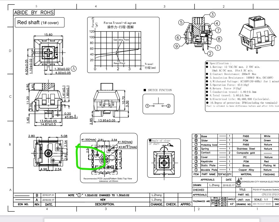
Unless the OP did so, no. The part was made to match the footprint in this data sheet

without a copy of the actual part so it may or may not be correct. A quick look now indicates the part doesn’t match the data sheet and is likely incorrect.
Peter
1 Like
Ahh ok. I’ll try my hand at editing the PCB svg and see if I can “fix” it. My part making skills are non-existent as already known ha.
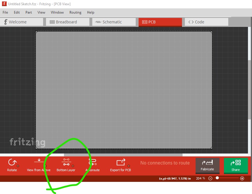
On a side note - as I know you make many parts, is it possible to specify that a part should default to the BOTTOM layer rather than the top? (In the use case scenario of these, they would be normally be mounted to the bottom/underside of the pcb, not the top)
Not as far as I know although I have also never tried. It is possible if you use copper0 as the pcb layer instead of copper1 it will default to the bottom of the board (you will need to swap the svg horizontally to be on the bottom of the board. If that doesn’t work you would need to use Inspector to set the part to be bottom of the board. The edit of the pcb svg should be fairly easy you should just need to move the pads around and silkscreen around. I can do it if you like, but if you have both the part and the key switch you are probably better equipped to do it. It is and was unclear to me how this thing actually connects to the key switch since the Cherry switches seem to have more than two pins and the data sheet doesn’t have an outline of where the switch is placed.
Peter
1 Like
I’ll take a look at switching copper1 / copper0 as well as editing the SVG. I stand far better chance correcting the existing part you’ve made than I do trying to make a new part from scratch ![]()
I know how to move a part to bottom layer etc, I just wondered if a part could be defaulted to bottom layer since when I place one of these, I 99% of the time will always want it on the bottom side, so would save me placing it, then having to set bottom layer. Part laziness but also part efficiency
I’m currently awaiting delivery of Kailh Sockets.
For what it’s worth, I have the Switches, I have a mixture of Cherry MX, OUTEMU, and Kailh, all of which have just the 2 pins.
Be cautious, test carefully, when creating a part like that. I suspect that a part using the bottom copper layer will be ‘understood’ to be mounted on the top. I do not think that is the same as having the part use the top copper layer, then telling Fritzing to put the part on the bottom. I expect that the 2 scenarios will be flipped left to right from each other. It it is only 2 pins, it might not matter. Anything else will likely end up wrong.
I have not tested this, so maybe it will do what you want. Verify carefully.
1 Like
Good to know thanks! I shall proceed with caution
@microMerlin is correct, setting the layer to copper0 doesn’t work. It loads the part on the top of the board but because I inverted the svg it is wrong when moved to the bottom. I’ll switch it around in a bit.
Peter
1 Like
This part may be closer. It by default loads on the top layer but if you set pcb like this it will load to the bottom by default
edit: replaced part with one with a correct pcb
edit1: which also turns out to be incorrect, deleted in favor of the correct part (by someone with the real part) below.
it may still be the wrong orientation though, the data sheet is both confusing and incomplete.
Peter
1 Like
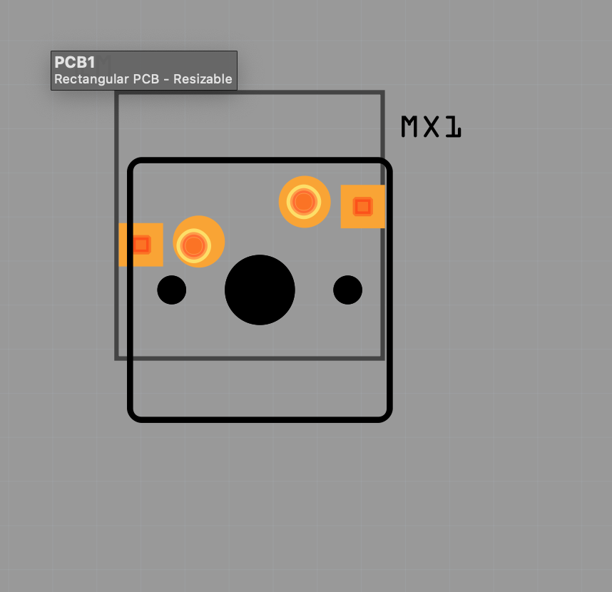
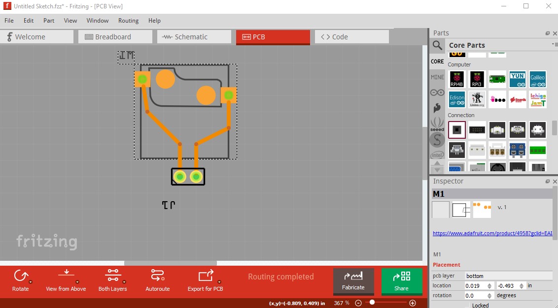
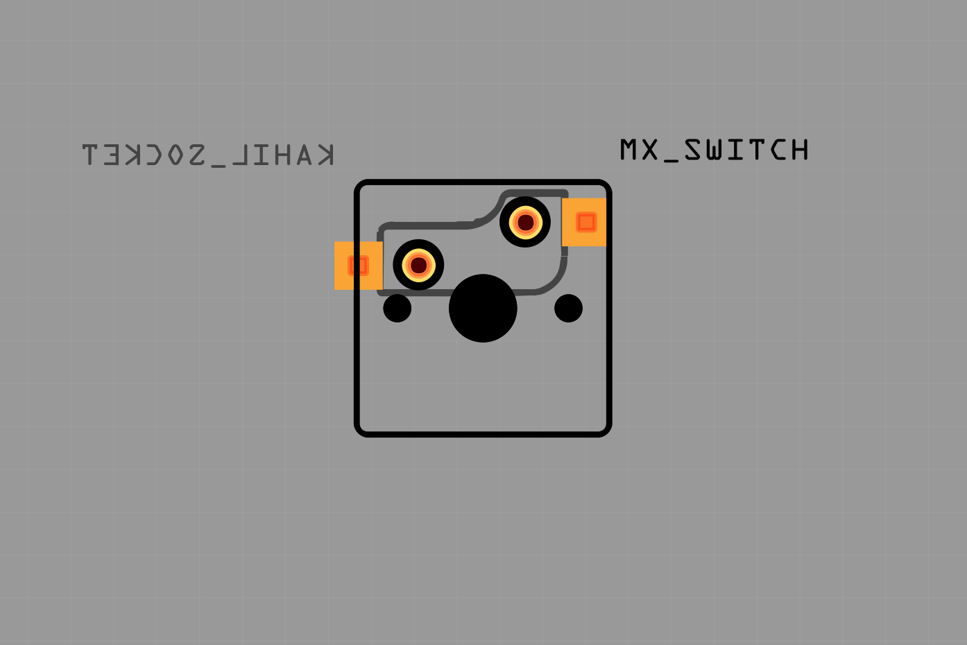
Funnily enough, this is as far as I’d got editing the earlier part… not great, but seems to be correct (within a few 100ths of mm)
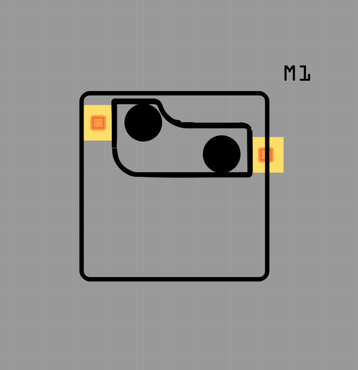
The circles are obv the holes of the kailh socket thing. The outlines are silkscreen - the larger outline is the Key outline, the inner outline is the kailh socket.
The one you just still has the contacts centred so with the outline is in the wrong position, or the contacts are, as the pins themselves are closer to the edge of the actual key if that makes sense
Kailh-switch-socket.fzpz (106.9 KB)
Interesting! This doesn’t match the data sheet for the key switch, but if it works for real parts then it is the one to use!
Peter
What datasheet are you using for the switch? (Or did you mean the switch socket?)
I’m using this as posted earlier: https://cdn-shop.adafruit.com/product-files/4952/4952_CPG1511F01S04-1-BOX_Red.pdf
The part I made lines up correctly with Adafruit’s Fritzing part from here: Make a Custom PCB with Fritzing | DIY Pico Mechanical Keyboard with Fritzing and CircuitPython | Adafruit Learning System
(They mention you too in that article!)
Edit: I just realised - to add to the confusion, my earlier screenshot was with the socket on top layer, when I should’ve screenshot it on the bottom layer!
That is the data sheet I used. It indicates the center of the switch outline should be 0.1in (2.54mm) below the center line of the bottom hole which is what I used. I just realized it is possible that is backwards and needed to be to the other hole though which may be the problem as I didn’t think to check the alignment of the pins.
editL Well other than the fact that I apparently forgot to do the 0.1in offset from the center line leaving it 0.1in to high in the silkscreen. If your image is with the part on top mine may still be wrong, as it is on the bottom and looks the same. This is with pcb corrected, I will replace the part above in a minute.
Peter
1 Like
EDIT: My mistake, mine IS right. Are you using mine or yours in that screenshot?
If i place my part on the bottom later, and then overlay the MX Switch on the top layer, they line up correctly (Other than Fritzings annoying ‘bug’ that means things don’t align to the same grid/position numbers. For example one component left = 2.000, second component left can only be 1.970 or 2.100. Manually setting the value it still jumps to +/- of the actual number I set (So annoying!!)
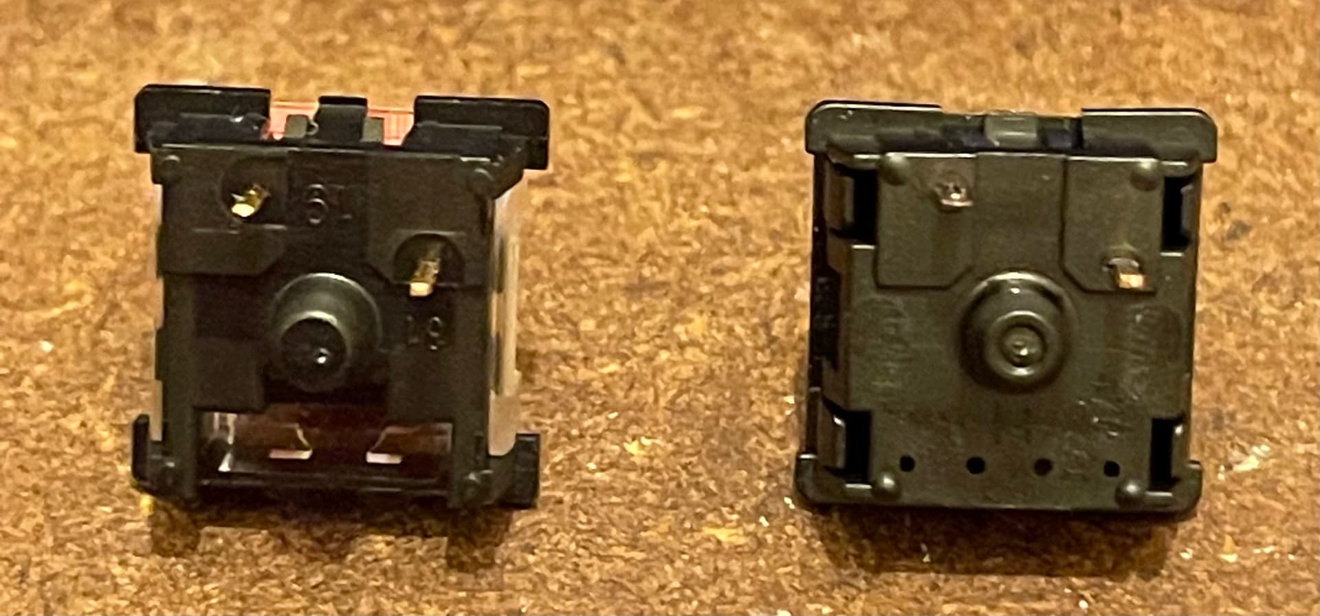
Switches: The one with 4 holes in plastic on bottom edge = Official Cherry MX, the one with a cut out area is OUTEMU
Original view of switch from underside
Flipped image as if viewing switch directly from above - so pin positions are correct to the MX_SWITCH in my fritzing screenshot, and thus, my socket on the bottom side is also correct if that makes sense
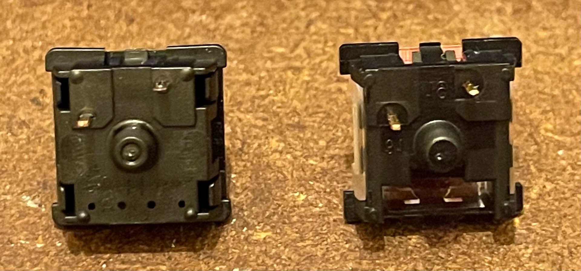
Although I may need to double check my exact measurements. Think I’ll make myself a test PCB via 3D Printing
The part above is my new one (which would seem to be wrong then.)
There is a fix in progress for that bug. It is caused by zooming (zooming out increases the inaccuracy) so zooming all the way in to the highest resolution available makes the placement more accurate and is an inconvenient work around.
edit:
I think I will just delete my parts and go with yours which are likely more accurate since I don’t have parts!
Peter
1 Like
Ahh interesting about the zooming bug - good to know a fix is in progress, it’s been an issue for a few versions.
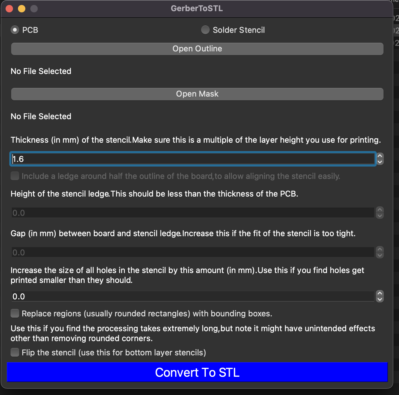
I’ve made a python program - compiled into an .exe for windows and a .app for macos that will convert the boardoutline & masktop gerber files into a 3D Printable PCB with holes - which means it’s a handy way to print out a pcb so to speak, and then place components in place with some tape/blu-tak/glue-gun - anything temporary if needed to see placement and hole size of components etc. I made it for testing custom components fitment and drill placements but obv will make the holes for all THT components on the PCB ![]() – So I will put together a test PCB, print it out and check the components fit as expected
– So I will put together a test PCB, print it out and check the components fit as expected
I plan to upload it here to the forum in the next week ish after some more testing.
I should add, I found a website that created 3D Printable solder-stencils (https://solder-stencil.me) and I basically adapted the code to work standalone (His web version uses DJango) as an app with a GUI - so the idea isn’t mine as such, however I believe I’m the first to use it to create printable pcbs for testing rather than solder masks (At least, that’s what the creator of solder-stencil suggested. I had some back and forth convos with him)
What an interesting idea! (3D printing a PCB)
… but be aware: 3D printers have huge differences related to tolerances (compared to normal 2D printers), and 3D printing a PCB as a way to “validate things” may be a not very good idea.
Regards!
Yes, I know this, I’ve been FDM printing since 2016, and MSLA printing since Jan 2021 ![]()
The hole size option can actually be used for +ve or -ve numbers to adjust holes accordingly. Also worth noting, that I resin printed my last test piece since it’s 0.050mm layer height and 0.051px accuracy so it’s actually super useful to test a PCB size ![]()