Hello
I’m completely new to electronic drawing software. I’ve always used pencil & paper, and lots of it! Sometimes I use AutoCad to produce a professional looking drawing at the end of the process. The whole thing is very time consuming, so I’ve been looking for some software to make things easier.
A new job has force me to try and update my old ways. I need to modify 3 PCB boards on an old machine at work. I also need to produce a schematic of the circuit.
Regarding the PCB:
The PCB is double sided, built last century and full of logic ICs. I have scanned the first board and have cleaned up the track image, see attached. I’ve been looking for a way of importing this track information into PCB software to produce a netlist.
I’ve realised that there is no easy way to do this in any of the software packages I’ve looked at so far. Dia was the closest, it had an import option, but unfortunately a bug prevented it importing SVG files properly.
I’ve resigned myself to having to input the PCB tracks manually in order to back trace the schematic, but any advice would be really appreciated on automating the process of inputting the pcb tracks from a graphic.
After learning a bit about Fritzing and spending hours reading the forum, I can see how versatile the software can be. I’m impressed, so I’ve signed up
Automated is going to be hard. Manual is possible, but the first item of business is going to be finding parts for all the ICs. We have some logic ICs but certainly not all of them. If you can find (or make) parts for all the parts on the board, you can move the parts in pcb view to match the above layout, then route the traces. From there Fritzing will produce the schematic (the traces will appear in schematic and breadboard which you probably don’t care about) as rats nest lines ready to be routed.
Thank you Peter,
I had planned to find or make the ICs as you said and place them. I’m having some difficulties at the moment with this, but I’ll start another thread to work through those.
What I’m looking for are ways to bring pcb track information and/or netlist into the software from outside (so I can add some automation). Can you or anyone share a bit of knowledge of how it works?
1, How is the track info is stored? I assume it’s in some kind of vector format with points, widths, shape, etc. Maybe similar to standard svg or gerber?
2, How is the Netlist info is stored? This is what I’m assuming is the info that shows which pins are connected together electrically. I’m guessing it’s a simple version of the above. Can you describe it?
It would be great to know a little more detail how the file system works. Using my zero knowledge of Fritzing, my idea is to edit the files outside the software, adding tracks, etc and then opening up the file in Fritzing again to show the imported modifications.
This parts creation tutorial may help. It has pointers to the documentation that exists for the structure of parts and deals with the underlying files rather than parts editor.
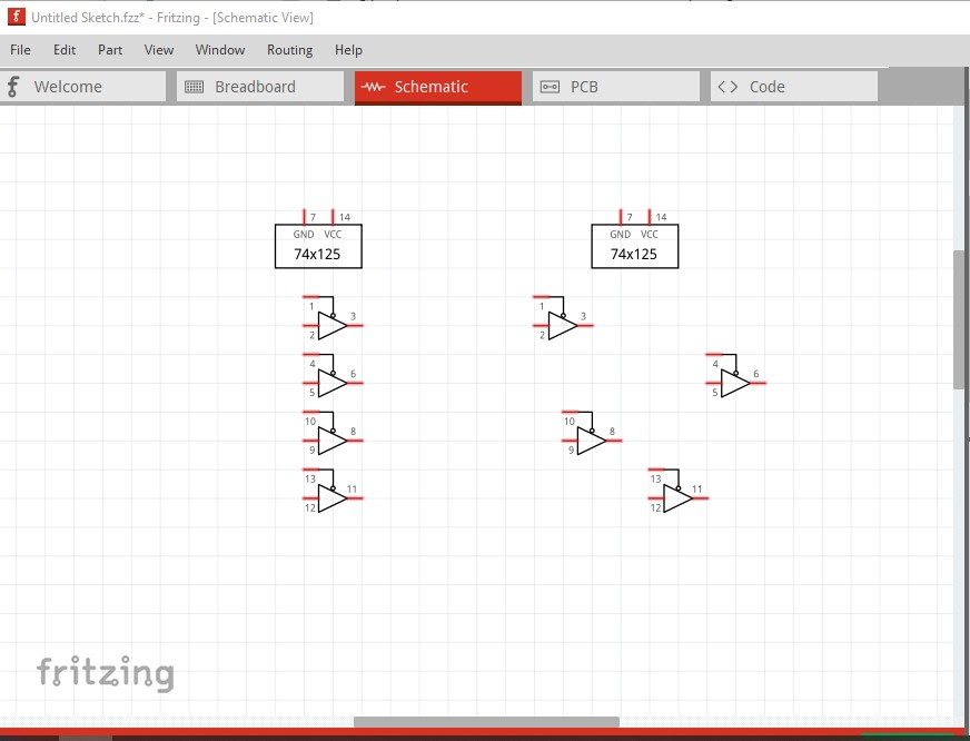
Part9 schematic subparts may be of interest as it allows (with a bunch of extra work in making the part!) individual elements of the part to be moved in schematic like this:
The part on the left is the default but you can click and drag any of the elements as seen on the right individually. This can make logic schematics much more readable.
This should be possible, but I’m guessing you will need to modify the code (which is not easy to understand) to do it. I can give you some pointers to where to look for things though. Every part has a unique moduleId defined in the part’s .fzp file. That is the primary index to everything, so to start you need to have all the parts you need defined (there must be another index value for different instances of the same part though.)
It is output (in the .fz file) as XML like this from this example sketch (the .fzz file):
I expect the exported netlist is generated from the above XML file (although I’m not sure of that!) Unfortunately the original developers have all left the project and there is very little documentation other than the source code (which is available on github) for how things work and no one who is very familiar with the code.
Assuming the image of the pcb (and hopefully the chips!) is all you have, I think you would need to first create a .fz file with the correct Fritzing parts present and then add the vias in their correct positions and then figure a way to associate the traces. I think it may be easier to do this manually though because associating the traces from the image looks to be a hard problem to me.
IF the top and bottom traces can be separated, it should not be too bad. Both autotrace and design rule check do variations of this strictly from bit map images. Following a bit map line to find out which pad / connector graphics it intersects with should be the same. Not efficient, but it works. The general technique used, is to render a single trace (identified by the “not copper” gap around it), then check for intersection with the rendered graphics for each connector, one at a time. All intersecting connectors become a single net list. Intersection is just whether “or” and “xor” result in the same image. If you have pixel counts for everything, it is an intersection if the sum of the total “copper” pixels in the separate pieces is greater than the copper pixels in the “or” image. To allow for “just touching”, one of the images is expanded slightly to force an overlap. That is what design rules check does, to locate separate traces that are closer than the configured minimum separation.
That does mean that the placed Fritzing parts must first accurately line up with the position on the PCB being matched to. In this case, smaller than normal pads (and holes) for the part footprints would help. Slight positions offsets would then be less likely to “short” to an adjacent trace while not affecting the generated net list. Since a complete duplicate set of part footprints is probably not practical, accurate positioning will be needed.
It looks like kicad (which is also open source) may be a better bet. They have something that converts a pcb image to a kicad .mod file. I assume you must have to assign parts to the resulting image somehow.
I have tried Kicad, but it didn’t seem to translate from pcb to schematic. In Fritzing you can modify or design in pcb mode and the rats-nest appears in schematic view. I couldn’t get this to work in Kicad.
Thanks for all the information. Sorry for the delay showing my appreciation, I’ve been packing for an unexpected holiday. I’m back on Friday, but I will study it while away, perfect holiday reading material!
Ah, I guess there work flow is schematic to pcb but not the reverse. I have a copy of kicad (I found both it and Fritzing about 5 years ago when CERN was supporting both) and liked Fritizng better because breadboard suits most things that I do (tie modules together rather than make boards.)) I think kicad is in much the same state as Fritzing: too few people willing and/or able to contribute code. Fritzing has a kicad footprint importer but it hasn’t had maintenance from around 2015 and thus doesn’t work on current Kicad (I wasn’t actually able to get it to work on old footprints either .) When last I looked a couple of years ago the kicad parts documentation was a work in progress … Then the easiest thing is likely to be to create all the parts and vias in pcb view, save the sketch and then try and add the connections in the xml file (copying attributes from a working sketch.) If that doesn’t work out it should be possible (if not easy!) to call the Fritzing routine that creates wires externally with the two end points (as if you had clicked on one connection and dragged to the other connection) to create the wire entries. This would need a development environment and figuring out the code neither of which are particularly easy (at least for me!) Schematic I fear will likely be manual. Fritzing tends to place parts on top of each other and you need to move them around til the rats nest lines show easy or at least feasible routing. I don’t know of a way to automate that although there may be one. Also it is best to make all changes in one view then switch to the others and route via rats nest lines. It is possible (and maybe a bug) to corrupt the routing database by making incorrect changes in another view. I have about 5 copies of this error over the last 5 years but have never been able to recreate the actions that cause the problem and thus can’t see if it is fixable.
I’m not sure which routine you are referring to. I can only see “Autoroute” which creates the pcb tracks (wires) automatically from the rats-nest.
I’ve been looking at how the .fz XML script works. Starting with just a generic IC placed in PCB view, I saved it and opened the XML file. Continuing in PCB view, I then added a wire between pins 1 & 2 and saved it under a different file name.
Comparing the two XML files, I can see that the added link also adds links in all the other views automatically. I assume this is done every time a link is added manually in any view. This could be a problem if I want to add PCB tracks outside of Fritzing. I was hoping Fritzing would add all the links in other views automatically when I opened up the modified file.
Also, I notice that every wire has the information about which pins are connected together electrically (the Net-List). Even the parts of wire, each section has start and end of the whole wire, along with the section info.
I’m now thinking that the only way to import PCB images to Fritzing is to convert it to a net-list first and import that. Associating the traces from the image is the hard part (as vanepp said) and microMerlin added some insight how this could be done, but I’m not sure which software to use for this.
I’ll study how the Net-List is stored in the XML first, especially for multi-point connections. Any help would be appreciated
Unfortunately nothing that easy , in the source code there will be a C++ routine that creates wires (which Autoroute will be using) given a start connection and an end connection. It should be possible (if not easy) to call that from an external program linked to the Fritzing source to create the wires. That will insure that all the parameters that Fritzing wants are present.
Yes, as I recall Fritzing calls routines to update the other 2 views whenever a change is made in one view. That is why I suggested it may be necessary to call the internal Fritzing routines to do the insert. It also likely does the updates to the internal SQL database during those calls.
Unfortunately I’m not aware of a netlist import function (although there may be one) so I’m not sure that will work. Fritzing will export a xml netlist but I suspect it creates it from the database, and I’m not aware of an import function although maybe someone else knows of one.
Edit: a late thought: it should, in theory, be possible to do this from the .fz file. All the information must be there to recreate the sketch, I don’t think there is anything internal although some of the parameters may be in the database which would be a problem. I’d make a test sketch with only pcb and a few wires (leaving breadboard and schematic as rats nest lines which is the simplest case) and try and change the various parameters in the .fz file to move things around and see if it works. The potential problem is that some of the parameters may refer to things in the database and thus not be setable to random values, but if that isn’t true you may be able to do this from only the .fz file which would be the easiest solution.
edit1: I think this may work. I created a sketch with two two pin connectors, then modified the .fz file to change the modelIndex to a different unique value (to see if the particular modelIndex is important!) The modified sketch loads fine so it looks like the modelIndex just needs to be a unique number in the 5000+ range (some of the lower numbers are hard coded in the Fritzing source.) That means you should be able to generate connections by adding connectors xml to the part that the connection is on (and the other endpoint.) Figuring out the geometry numbers may be somewhat exciting but with DIP packages as you have I expect trial and error should allow you to get the needed offset to each pin connector by making a connection and calculating the needed offset from the geometry of the original part. The Z may be harder because I don’t know what it does. Hard, but very likely easier than figuring out the Fritizng source to get it to do it for you . Here I my two test files TestSketch2.fz is the original two 2 pin connectors and 2 wires file. I then did this translate on the modelIndexs to create TestSketch3.fz which as far as I can see renders correctly.
the first two modelIds aren’t connectors and were left alone, the bottom 4 seem to be the two ends of the wires and were changed to the number after the *.
Z is for ordering, to show what is drawn above and below other elements in the view. Mostly important (for wires) in breadboard view, since that changes the way it looks. In other views, there is no real difference in the order of the wires. Just need Z in the appropriate range, so that wires are above the pcb board itself. I don’t think there are any Z ordering occlusion issues for schematic and pcb views.
Thanks, I just read your messages this morning. Yesterday, I had a good play with .fz XML and worked out how to add netlists in the editor.
It worked in a different way to what I was expecting. Basically, after placing your components, you can add a wire at the bottom of the XML (stating the start & end connection). When opening in Fritzing, the Rats-Nest appears in the other views.
So far, Fritzing has done an excellent job at correcting in the rest of the XML above the wires. The actual wires were drawn in the wrong place, but I “wireFlagged” them to appear in the breadboard view (as I don’t use this view). The Rest-Nest however, appeared in the correct place in the other views.
To draw on the Schematic view set wireFlags=“128”, Breadboard wireFlags=“64” and PCB view is wireFlags=“4”.
The great thing I found is that I could add several connections to one wire and Fritzing would show the Rats-Nest for all of them. Not how Fritzing would construct the XML, but it reads it ok. The following joins pins 2, 4 & 13 together;
So, I now have a way to import the Net-List connections. I just need to find a way to get the connection list from the PCB image. I guess I’ll start manually and see if I can find a way to automate any of the steps.