Hi. I am trying to design a circuit, part of which will be a prototyping area. This area will have a matrix of through holes linked together in 3s. I can build the circuit OK but I want to show the linking on the silkscreen. I can see in Part Inspector that it is possible to add an image from a file but I don’t know how to make the image. Is there a program that you know of that will enable me to produce an image file that has accurate dimensions? What file type would be best, .jpg, .bmp or something else?
Thanks.
Generally preferred is .svg format, and you can use Inkscape to create it. Just make sure to set ‘real’ units for the image dimensions, so that Fritzing can scale it properly to match the dimension being used in the sketch.
Thank you. I’ll give that a try.
If you are new to using Inkscape this tutorial set on making parts (which uses Inkscape) may help. You could also do this by making a custom part that has only pcb view (no breadboard or schematic) for the breadboard area.
Peter
1 Like
Thank you, Peter. There is a lot of information here, it will take me a while to work through it.
It may be easier to let me either create a part or an svg with what you want (for which I would need the layout of the prototyping area with number of rows, number of columns, pitch, (i.e 0.1in pich or 2mm pitch), interconnections (i.e. the 3 pads connected together), desired pad (circle, ellipse) and the size of the drilled hole (typically 0.038in for 0.1 headers) and the desired silkscreen. If you aren’t already familiar with Inkscape using it is also fairly complex as is parts making.
Peter
Hi, Peter. I did reply but I did it via the e-mail message I received and I suspect it didn’t get to you.
I think it would be most useful if you could make a part that has only 3 interconnected holes. I could then arrange a matrix of these to any area I might wish to make in the future.
The holes need to have a pitch of 0.1in, have circular pads and 0.038in holes. The 3 pads would be connected together in a horizontal line and the silk screen would show the track connections.
Thank you,
Chris.
I may have missed it (I tend to delete the email notices from Fritzing figuring I have read it in the fourm though!) Here is a part that should do what you want. It is only pcb (no breadboard or schematic) and has a part label (because I can’t figure out how to suppress it in the part!) which you can hide like this:
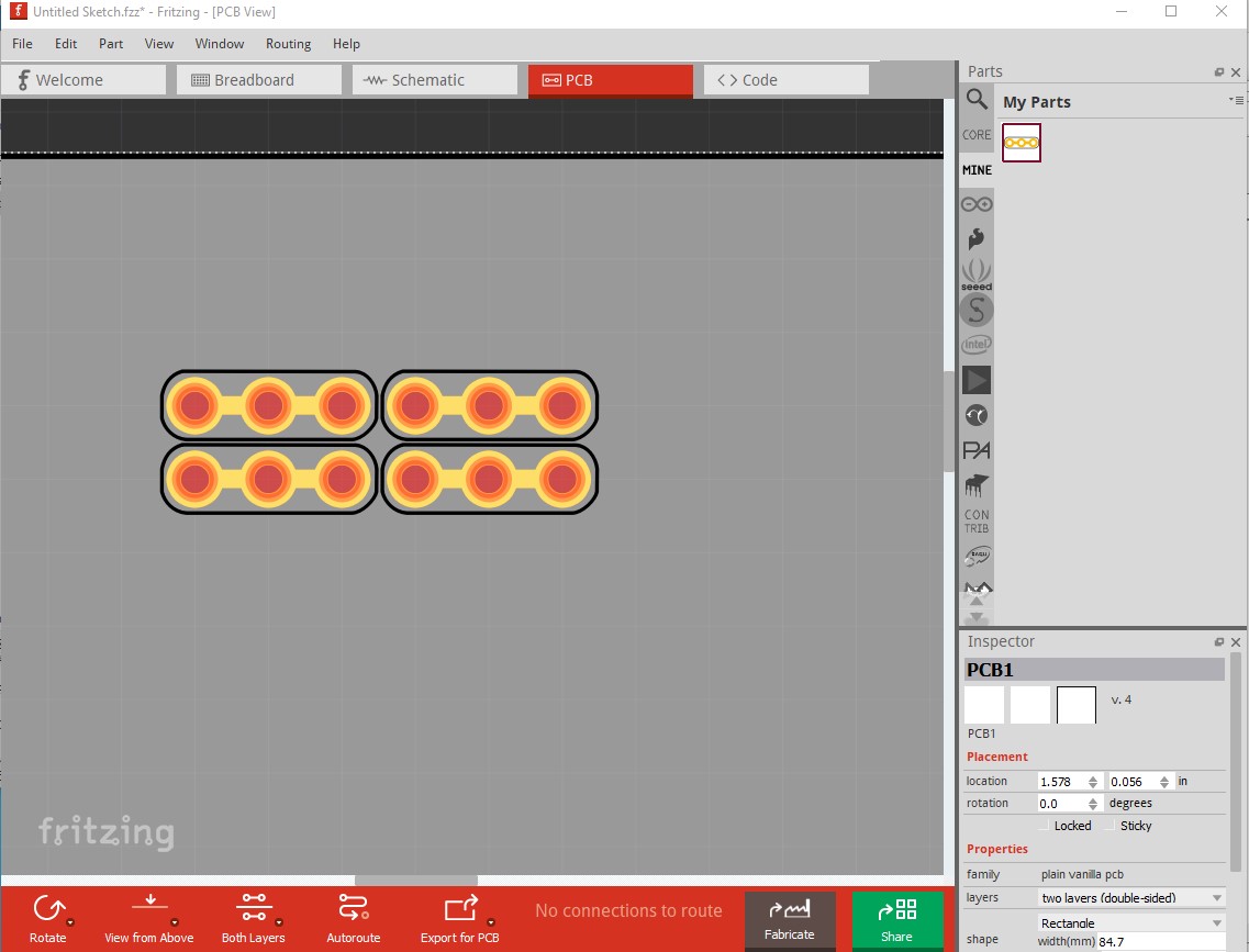
(this is 4 copies of the part arranged on 0.1in boundaries horizontal and vertical)
by doing this:

if you click on hide here it will suppress the part label. Here is the part:
three-pad-proto.fzpz (2.2 KB)
You can rotate the part 90 degrees to get a vertical version.
Peter
Thank you, Peter, that looks just what I need. I’ve not got time to try it at the moment but will do as soon as I can.
Chris.
Hi, Peter. I’ve tried it and it works great. Thank you.
Am I correct in believing that the holes are through plated and the tracks are on both sides of the board?
Chris.
Yes, and the hole size is set to 0.038in suitable for 0.1in headers as well.
Peter
The copper traces are on both sides of the board, which I did not expect, and holes will be plated through. However, A test says that Fritzing does not know that the holes are connected. I think a bus entry is needed, and maybe dummy breadboard and schematic views. Getting internal connections for a pcb only part could be a bit tricky. To get ratsnest wires in the other views.


Side note: The pcb silk screen for the resistors IS in the exported svg, but it is invisible here. It is white on white.
It is bused now, but it looks like that isn’t propagating to schematic (probably because schematic doesn’t exist in the part.) I tried making it a breadboard (so as to make it work in schematic) but then it renders but won’t select in pcb and thus you can’t move the part in pcb view, so I left it as pcb only as the only workable solution. I think this is as close as we can come with Fritzing.
Peter
Hi, Peter. It does what I need it to do. I will not be adding components to it in Fritzing, I just need to make a bare PCB to be populated as required at the time.
Thanks.
Chris.