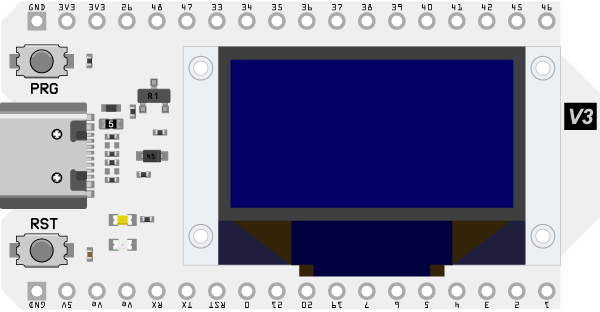
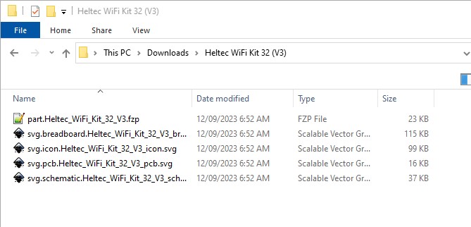
Yep, the new file appears fine so all should be well.
Peter
Yep, the new file appears fine so all should be well.
Peter
I just wanted to say thank you for making the fritz file for the V3 module. A huge help, I wanted to ask if you could put something else together…https://www.amazon.com/Screw-Terminal-Breakout-Module-BeagleBone/dp/B08LKBKCDY.
I need this for a project and I tried to make it myself not working well any assistance would be appreciated!!
The B08LKBKCDY module looks like a lot of work, certainly for me because I have nothing like that upon which to build. @vanepp might be the man for that job… if he has the capacity…
Thanks for the recommendation @UniquePete! @vanepp if you could please look into this it would be very much appreciated, I am very new to this software and this build would be great for a group of us using these. Thanks again!!
A part will be up in a bit.
Peter
Thank you, I really appreciate it. Let me know if you need any additional details.
OK here is a part that should do what you want. I suppressed pcb as it doesn’t appear useful as this is a shield and it is set that if you stack it on top of a beagleboard black (the Adafruit one I believe) in breadboard it will connect to the shield in schematic (you however may not want that once you see what happens in schematic ![]() .)
.)
Screw-Terminal-Block-Breakout-Board-Module-for-BeagleBone-Black.fzpz (22.5 KB)
Peter
I really appreciate it, huge help! Looks great!
Once again, I figured this was the best place to keep adding Heltec parts. I have run this one through FritzingCheckPart.py.

Heltec WiFi Kit 32 (V3).fzpz (34.6 KB)
Oh Jesus this is exactly what I needed! Thanks a lot!
Could you explain me where are the inkscape commands to modify the PCB part?
I only found those to modify the schematic and in the XML list I didn’t found any PCB references.
The pcb items are in the pcb svg. There are typically 3 (sometimes 4) svgs in a part, breadboard, schematic and pcb (and optionally icon, often replaced by the breadboard svg) as well as the fzp file (which ties them all together.) In this case unzipping the fzpz file gives this

the pcb svg is svg.pcb.Heltec_WiFi_Kit_32_V3_pcb.svg
which looks like this in Inkscape
Peter
Oh gosh!
I took for granted that Schematic and PCB was all in one file, like in Fritzing…
Thanks, now it’s clear to me why I couldn’t find… what isn’t there
Parts creation takes more than a bit of getting used to. There are also interactions between the fzp file (which is XML and describes or refers to elements in the svgs) and the various svg files as well as rules for layout. It is uncomfortably complex to make parts. I believe there is ongoing development work to finish parts editor (it was incomplete when development stopped in 2016) but that hasn’t been released yet (and is a large part of the reason I don’t use parts editor!) FritzingCheckPart.py helps by checking for and flagging the common errors.
Peter
Not me, but I believe it’s available in this thread.
Hi, I created a fritzing part for the “Wireless Tracker” board from Heltec, it was a nightmare considering it was my first fritzing part and the measurments for the pin spacing is a bit off but here is my take on this part.
HeltecWirelessTracker.fzpz (22.8 KB)
This tutorial will give you guidance on making parts which should help you clear up the issues. I’ll have a look at your part when I have finished fixing up another project.
Peter
There isn’t very much wrong with your part. As you said the pin spacing is a little off but over all the part works fairly well as it. The first issue is that breadboard doesn’t have a layerId. As a result your part in a sketch will not export as an image (that is the only thing I know this affects but there may be others as well.) It needs to match the layerId in the .fzp file for the part which will usually be “breadboard” and be the top layer group that contains the entire svg
original svg
corrected
Then I looked over the breadboard svg (I’m using Inkscape here, it looks like you are using Illustrator?) The first thing I did was grab this png from the heltec site and imported it in to Inkscape
then scaled the png so the pins matched the connector on the board.
I actually sized it via a 25 pin male header from Fritzing which will be the exact correct length. The I selected just the board, locked height and width then set the size to 65.48 mm (as the listed size on the Heltec web site.) That make the board a little long to the listed length, but I left it alone because it better matched the size of the image.
Then I created a standard header pad that matches the Fritzing 0.1in header definition
then moved that to near the bottom left connector (which by Fritzing convention is connector0pin.) I selected the current pad at that position and noted its its x and y coordinates
then I moved the new pad to the same position as the original pad like this
and deleted the old pad and added the square that is on this pin.
and moved it on top of the connector.
Then I selected the circle that is the pad and duplicated it then clicked the + tab on the x icon to move the pad 0.1in in x
this is the easiest way I know in Inkscape to correctly space connectors (at least 0.1in connector!) You can also do so by adding the appropriate increment to the x coord and then copying the new value in to the x coord (useful for 2mm connectors!)
then ,move on to the connectors on the top
now replace the text rendered as paths with text (as it is easier to modify if you or someone else needs to modify the part!)
The labels for the pins are set as text (desirable) but have had their font size (likely by Fritzing because the px was left on the font size which Fritzing reacts badly to!) reduced to very small so set a larger font size to recover the text.
now we are done so set the layerId by selecting the entire svg and grouping it
then set the first connector to connector0pin with all the pins being after that at the bottom of the svg. The reason for this is that I have a script which will read the svg and renumber the pins in sequence (laziness at work!) The output from the script looks like this
I then used Randy’s Inkscape extension to create a Fritzing schematic svg for the board, then copied the breadboard svg in to pcb, and edited it to delete all the unneeded components and text and made the appropriate groups for pcb. I then created a .fzp file and labeled the pins then added buses for internally connected pins which resulted in this part which implements the board.
HeltecWirelessTracker.fzpz (13.3 KB)
Pretty much everything I did here is covered in this tutorial (if you haven’t already seen it)
Hopefully I haven’t scared you off and we will see more parts from you ![]() .
.
Peter
Here’s the latest version of the Heltec WiFi LoRa 32 board (V4).
Heltec WiFi LoRa 32 V4.fzpz (74.8 KB)
I see that the Heltec Wifi LoRa V2, V3, and V4 have been created as .fzpz and I wanted to thank you all for the work you put in on it! I am working with the V3.2, ESP32S3. Has anyone done this device yet?