Heltec Dev Boards

Hmmm … Maybe we should do some collaboration. I’m comfortable with the technical details of creating parts, and can do the line style diagrams for schematic and pcb. I can create functional breadboard parts, but am no good at making them (or icons) actually look good. See the recent post for Dragino LoRa Shield part creation for a sample. The graphics in that that look any good, I copied from someplace else. Or created from dimensions and straight numbers. I edit the svg files with a text editor, not using Inkscape, Illustrator, Corel, or any other graphics program. That way I get the pieces exactly where I want them based on coordinates.

Hey Pete,
thanks for working on it. I actually only need it for the breadboard view. I just want to illustrate a little setup with the Wifi Kit. Therefore, an illustration would actually do it for my purposes. I don’t need the PCB view.

Try this.

Heltec_WiFi_Kit_8.fzpz (24.3 KB)

1 Like

Thanks man, this looks perfect! I really didn’t think that somebody would help me out this quickly.

That was pure luck, really :innocent:—I had just completed another project and, because I work with Heltec stuff a bit and had already done the other parts, everything was pretty much there. I’m not usually looking for things to do on a Sunday afternoon… :sunglasses:

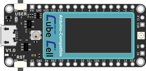
Here’s the new Heltec CubeCell Dev-Board Plus for anyone who might be interested too.

Heltec CubeCell Dev-Board Plus

Heltec CubeCell Dev-Board Plus.fzpz (58.1 KB)

2 Likes

Amica NodeMCU DevKit.fzpz (50.7 KB)

The holes are too small the amica NodeMCU do not fit

Is it the header pins that won’t fit in the holes, or are the holes in the wrong place? I just used the ‘standard’ pads provided in the Fritzing template, and the pin spacing should be exactly 100 mil—I use the part primarily for documentation, but it fits perfectly on the Fritzing breadboard, so the spacing shouldn’t be a problem…

The holes are too small and the device do not fit, the pins cannot enter the holes

Look the picture linked here http://gloglos.com/sharedimg/IMG_6410.jpg the green was created with your design, but it is unusable unfortunately.

Like I say, I just used the pads provided in the template file, and visually, they sit neatly over the pads on the module. But if it doesn’t fit, it doesn’t fit… Just looking at a few other parts in the Fristzing library though, mine are not the smallest header holes, but I can also see that others are larger. The pad diameter I use in all of my parts is 1.118mm/0.044in (per the template), but I can see some parts with pads that have a pad diameter of 1.447mm/0.058in.

I wonder if anyone can advise what pad diameter should be used for a ‘standard’ pin header? If that’s something other than what I’ve used, as it would appear to be, I’ll go back and update all of my parts.

I must confess that I generally use Eagle for PCB layout and just whatever the default hole size happens to be there, which is actaully a little bit too big for a snug fit.

it would be nice if you can change the holes to 1.447mm/0.058, I will do a prototype test for you and confirming the outcome for the good use of everyone.

I am limited to 3 replies only so I reply here:

Excellent, I will send it for production it will take a week more or less :slight_smile:

Ordered, I will get you posted with information and pictures if it fits

See how you go with this one (pads 1.447mm/0.058in).

Amica_NodeMCU_DevKit_1.0 (v2).fzpz (56.8 KB)

1 Like

The problem is that the svgs are dimensioned in px and thus the gerber export is the incorrect scale. I’ll correct that and post a corrected version in a bit. The holes in the pcb are not on .1in centers due to the incorrect scale.

Peter

Thanks @vanepp.

As you know, I use Illustrator to prepare my files, and we’ve encountered this problem before [in a slightly different context]. Having now looked a little more deeply into this problem, one solution that’s been suggested is to simply change the ‘px’ unit (which, in Illustrator, is 1/72") in the SVG file to ‘pt’ (which, I believe, is universally recognised as 1/72"). The files open OK, but I can’t quickly see if the that fixes the present problem.

@vanepp, I’ll be very interested to see what you come up with. Changing the units to ‘pt’ doesn’t seem to make any difference (you’ll probably know immedaitely why that is).

As best I can determine from the Gerber files, though, the drill hole being specified [for my original part] is 28 mil, which on boards that I have at hand seems to take a normal pin header snugly, but without needing any force—I do normally specify a drill size of 1mm (~40 mil) for a header pin (the drill holes generated for the larger pads I created in the above part are ~41 mil), but there’s plenty of ‘spare room’ in those holes.

The variation in the separation between holes only appears to be in the fourth decimal place (i.e. a tenth of a mil), which I would have thought would have little impact.

Yes, the problem is that you need to change the drawing units from px to in. As part of that Inkscape redoes all the internal sizes. I don’t know of a way to do that in Illustrator, reading their documentation I’m not sure it is possible (although Illustrator appears to process a svg that is dimensioned in inches just fine.) They seem to think they know best and you should just use what they give you (although there may be some way I don’t know to set the values as well.) Here is a fixed up version of the part and what I did to get there. Since I was doing it anyway I converted everything to meet the graphics standards as well as fixed the pcb svg.

breadboard:

Mostly just rescaled this so 1px = 1 thousandth of an inch. In Inkscape this is described here:

again I don’t know how (or if!) this can be done in Illustrator. As well the connector0pin is set as a group rather than on the path drawing element, since I needed to ungroup the svg to rescale it, I moved connector0pin to the path.

Schematic:

Changed the line colors to match the graphics standards and changed the terminal definitions to a 10 thou by 10 thou rectangle.

pcb:

FritzingCheckPart.py complains about the drawing units being px (which can cause scaling problems):

Warning 19: File
‘svg.pcb.Amica_NodeMCU_DevKit_1.0_pcb.svg.bak’
At line 4

Height 134.363px is defined in px
in or mm is a better option (px can cause scaling problems and likely did here from the example board above!)

Warning 19: File
‘svg.pcb.Amica_NodeMCU_DevKit_1.0_pcb.svg.bak’
At line 4

Width 70.3px is defined in px
in or mm is a better option (px can cause scaling problems!)

This corresponds to this in the xml (and in Inkscape):

The red circled height and width in the first line of the xml are the problem. If defined in px, then Fritzing guesses which of 72dpi or 90dpi was used on the original and sometimes gets it wrong (especially now when the newest svg standard is 96dpi!) As we see in this image the pins are not on .1in boundaries (because this Inkscape is using 96dpi.) The blue grid lines are on .1in boundaries. So I figured out what they should be and scaled them to that. X pad to pad distance should be 0.9in, currently they are 0.671in,

determined by setting dimensions to in and selecting the bottom left pad with a X offset of 0.006in and then the right bottom pad:

which is at 0.677in (but should be at 0.906in!) So scale up by 1.341281669150522 in x by setting the width from 100% to 134.1281669150522%

Which widens the X dimension (while distorting the Y as we haven`t changed it yet!) so that the pads are now spaced exactly 0.9in apart as desired. Now do the same in the y (height) direction changing height from 100% to 133.8432122370937%.

The original size of the board was the outline circled in red, the new size (as we see from the grid lines) has the pads in the correct places. Now we need to resize the drawing to reset the view box, and change the dimensions from px (editor dependent) to in (fixed) which has the effect of changing all the internal values and setting the height and width to in in the xml (circled in red here):

With a few more changes (scaled up to the standard scale and clean some things up a bit) this is the pcb svg in the new part. As before, I don`t know how to do this in Illustrator or if it is possible though. I changed all the pads to be standard .1 header pads, that is the hole is 0.038in and the ring thickness is 20 thousandths. This should produce a correct pcb for the original poster. Note that if you want the mounting holes drilled, you need to drag a hole from core parts pcb over the mounting hole in silkscreen in the sketch and adjust the size of the hole to match the mounting holes, by default the mounting holes are not drilled.

Amica NodeMCU DevKit 1.0-improved.fzpz (40.0 KB)

Peter

Thanks @vanepp, but I’m not sure we’re identifying the real problem here. The dimensions are all as we would expect inside Illustrator, where one works in inches or mm as one prefers (not in pixels), and there are clearly some problems importing Illustrator SVG files (which insist on presenting dimensions in Adobe’s idea of pixels) into Inkscape.

But in creating my parts, I use the Fritzong Parts Editor to do the initial compilation of relevant files. Now, the Parts Editor may be a bit flakey, but it does the original translation of the Illustrator SVG file and converts from pixels to inches. Unfortunately, the present example is not the best to be discussing here (we’d really need to go back to the original part), because I just modified the SVG file to increase the size of the pads, and didn’t then go back through the whole ‘construction’ process. As a result, the dimensioning inadvertently reverted to ‘Illustrator units’.

But the Fritzong Parts Editor, I would suggest, correctly translates Illustrator’s pixel dimensions into inches, using a scaling factor of 72. That translates the original 134.363px x 70.3px dimensions into 1.86614in x 0.976389in (although this conversion suggests that the scaling factor is just 72.00—i.e. correct to only two decimal places), as can be seen in the original part file.

Quite apart from everything else, in the Inkscape example you present, that translation does not appear to be symmetrical or as accurate—the scaling factor on the X-axis appears to be 71.59, while on the Y-axis it’s 71.32. I am guessing that this translation is automatic, but I would have to ask why the X-axis is being scaled differently, albeit only slightly, to the Y-axis? And looking at the PCB SVG in the ‘improved’ part, the scaling seems to be different again.

The scaling does seem to be the main problem here, at one level at least, but I’m not sure we’ve identified the source of this problem.

You are right, there is something else going on here. I just ran your original part through gerber processing and while the holes are too small (0.028in) and the spacing is a little off, but it is not as off as far as the picture of the boards:

From the gerber drill.txt file from the original part:

X021160Y017739
X012222Y017739

X .8938in (should be .9in)

X012222Y016743
X012222Y015748

y 0.0995in (should be 0.1)

X012222Y014752
X012222Y013756
X012222Y012760
X012222Y011765
X012222Y010769
X012222Y009773
X012222Y008777
X012222Y007782
X012222Y006786
X012222Y005790
X012222Y004795
X012222Y003799

So there is something else going on. @marcellodipietro how was the broken pcb made? Generated the gerber files and made by a board house, or printed and hand etched? The part looks mostly right, or at least not as wrong as the boards indicate.

Peter

I thought this post was going to appear above, with the posting of my modified part, commenting that it should not be used. In the event, it just appears down here, in sequence. Nonetheless, my apologies for trying to shortcut the process to generate this part. The following includes the bigger pin holes and uses the correct scaling:

Amica NodeMCU DevKit 1.0 (2).fzpz (56.3 KB)

As it is based on my existing artwork, it would be the basis for any further modifications I might make. If you don’t care about anything else I might do, then you’re probably just as well or better off using the version created by @vanepp, since he’s been playing this game much longer than I have and his part will be entirely consistent with Inkscape, rather than Illustrator.

Also, further to another comment I made above, I have no problem fitting female headers in 28mil holes, but I note that the male header pins are indeed larger and so require a larger hole (per these latter versions of the part).