I am new to fritzing and looking to do something that I believe should be very simple but I cannot figure out how to make work.
I have some 100mm x 75mm copper clad PCBs (https://www.amazon.com/gp/product/B01LZVMIBN) and I want to etch four 25mm x 25mm rectangular touch pads into the top layer of these boards. I then want to route traces to a set of four female header pins to go off the board to read into an MPR121 controller chip.
Upload the .fzz file of your sketch (upload is 7th icon from the left in the reply menu) and one of us will look it over and probably tell you what is going wrong.
I attached a basic board, which I don’t think is what I actually want. I used four solder pads as the capacitive touch pad, but I think I just need to etch around a rectangle to achieve the shape I want isolated from the rest of the board. Is there a better way to etch the shape of a rectangle and route that to a pin?
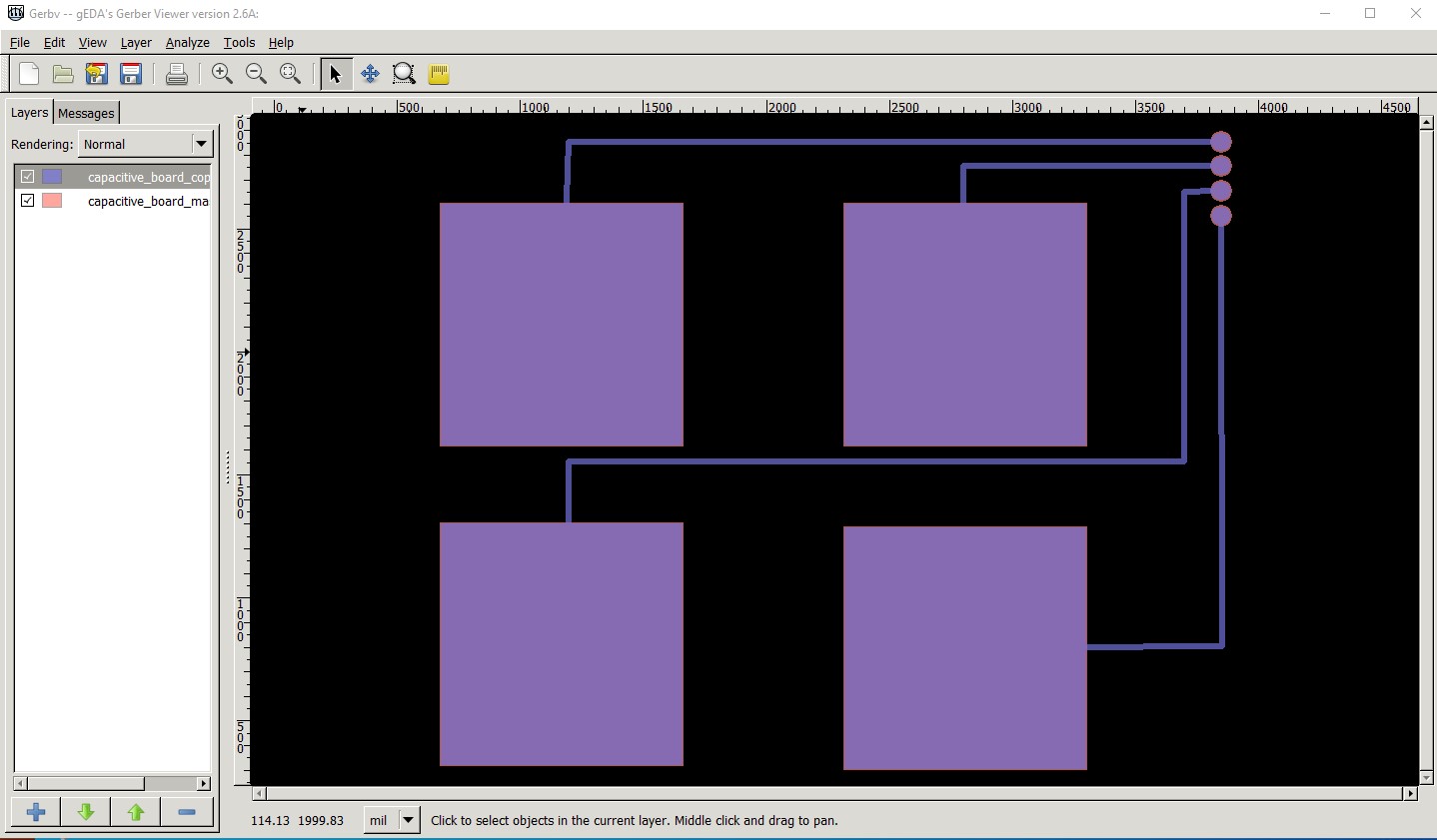
Here you have 4 copper pads (without solder mask) and traces connecting to the 4 header pins (and the traces have solder mask). As far as I can see that is what steelgoose was suggesting and intending. What do you want different? Are you trying to eliminate the holes for the vias? Pads1 and 4 don’t have holes now.
Okay, interesting. Maybe this is what I am trying to do. This is my first try making a pcb, so just looking for confirmation that this is right before I order a set of these, or try to mill them myself on a desktop milling machine.
I have a set of 100mm x 75mm copper boards and I am trying to etch around the rectangular capacitive pads and route to pins at the edge of the board where I can solder some header pins to the board. I just put a rough design together of what I want the final product to look like (without the traces from the pads to the pins).
Yes. The black in the image 2 above is bare board (covered by solder mask.) The light purple is exposed copper (in the pads) with the copper mask starting around the edges. The traces are slightly darker purple to indicate they are covered in solder mask. So this should show up as the 4 desired bare copper pads with solder mask covered traces to the 4 header pins as desired.