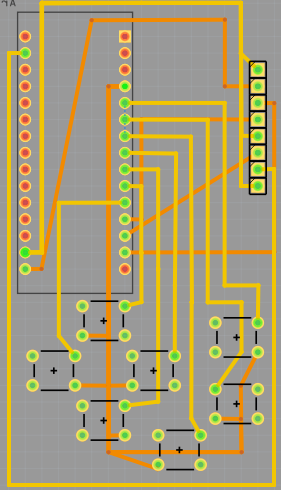
I am a begginer of doing pcb, and i would need help from someone who know this well to confirm if my connections are good in my pcb. The big thing in the back is an Arduino Nano v3, the 8-pins in the front at the right are pins for a screen : 1.44" Red Serial 128X128 SPI Color TFT LCD Display Module – phillipjfry and there are seven button in the front down.
Untitled Sketch.fzz (17.1 KB)
Your best bet is to upload the sketch (the .fzz file, upload is 7th icon from the left in the reply menu.) It is hard to do anything with an image.
Peter
ok, thanks, i’ll do it right now. And yes, i know, the 8 things at the right are antenna, but it was all i got for 8-pin for my screen.
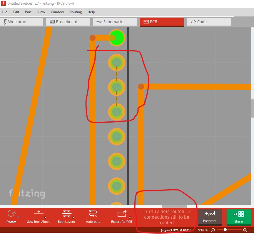
There are a couple of problems with your layout. It doesn’t pass DRC (routing->design rules check) in pcb:

because the wire circled in red (with the top copper layer view disabled here) is too close to another wire. Easy to fix by moving the wire a bit.
also routing is not complete (indicated by the more nets to route message at the bottom of the screen) and several pins on the Nano are shorted together which they likely shouldn’t be. That is likely caused by the short between D2 D3 and D4 in schematic. I would advise routing schematic completely to make sure the schematic looks like you expect it to. It is very easy to make routing mistakes in pcb which in Fritzing will show up in schematic and breadboard views.
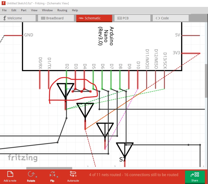
In this case you look to have wiring errors in breadboard and schematic that are reflecting in to pcb and breaking your layout.
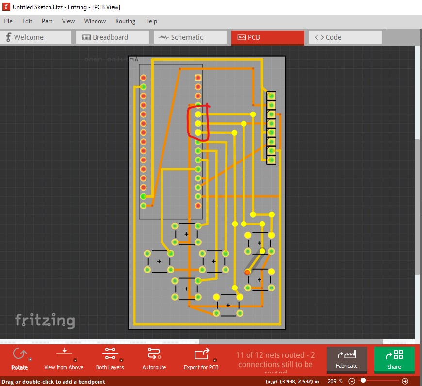
Here in pcb I clicked on on of the nano pins which lights everything Fritzing thinks is connected to it yellow. As you see three of the wires (circled in red) are shorted together. To fix that I move back to schematic and clicked Routing->select all traces, then pressed the delete key to delete them all. Then I did the same in breadboard. That looks to clear the problems in pcb and moving the wire that is too close makes DRC pass.

Note this only indicates that Fritzing no longer sees any problems in pcb, it doesn’t guarantee that the board is correct. As to your antenna parts, I remember (but can’t immediately find) a Fritzing part for this color display. If I can’t find the copy I remember it is easy enough to make a new part. With that I would suggest actually physically building the circuit on the breadboard, and run the code to make sure the circuit works as you expect before ordering boards. I’ll either find or make a part for your display and post it.
Peter
Thank you so much for your answer, i’ve asked on two other forum, but they all tell me to add thing such as a ground copper pour, place the buttons in a more special way, etc, without answering my question. But you anwer exactly what i wanted to know without changing everything. But i have another small question before doing it : is it ok for the buttons that the 5v is coming from the front layer and the gnd from the back layer, or it must be on the same layer?
The front and back layers are identical in pcb so connections from either side are fine. If you wait a while I will upload a part for your tft display so you can replace the antennas with a correct part. The part I remember isn’t the same so I need to make a new one.
Peter
Ok, thank you again very much!!! Take your time, no stress.
OK here is the part for your lcd display to replace the antennas.
1_44in-color-tft-display.fzpz (5.1 KB)
with that you should be good to go.
Peter
Thanks you a lot, bye! ![]()