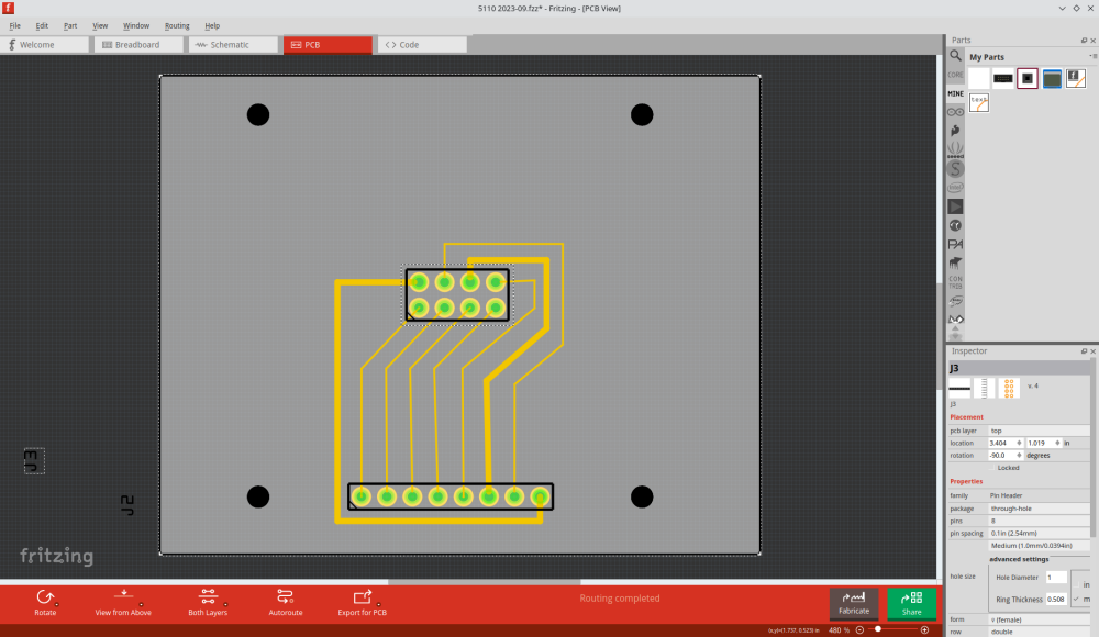
The PCB shown below is to connect and hold a Nokia 5110 LCD screen. The spacing of the holes relative to the 1x8 set of pins is crucial to the design.
If I were able to group the holes, then I could treat them as one object and align that with the PCB. Then, after grouping the holes and the PCB, I could treat THAT as one object and align the pins to its center.
Your best bet would probably be to use the Nokia 5110 part available here:
I don’t remember if the mounting holes are in the part (likely they are on silkscreen and you have to drag a hole over them if you want it drilled.) An alternative would be to make a new part with the holes drilled. That should do what you need as the holes will move with the part.
edit:
I had a look at the listed parts and neither my original or the modified blue one are correct. If you would like a part with the mounting holes drilled please upload your sketch (or the size of the 4 holes and their positioning relative to the header) and I can make a corrected part for you.
I knew I should have made my example more general. Grouping would be useful in a lot of cases, not just the 5110. I’ve wanted it several times over the life of this project.
Unfortunately it is easiest to do in a part, in a sketch is more difficult I expect. You can select an area with a select box and move it, but everything in the select box (which would include your double row header in this case) will move, and you have to redo the select to move it again. I expect that grouping things in an area (or being able to select them to add to a group) to be difficult to achieve.
edit:
You could also open an enhancement request here on github:
for what you want, although as noted I expect it will be judged to be too much work unless it is really popular.