Your SO5V1000 part has a number of problems. I ran it through FritzingCheckPart.py which flagged the following errors (there are a bunch of warnings as well, but the errors are by and large the important part):
Error 18: File
‘part.EasyPower_SO5V1000_8f2806aad67f3da3bb87188cc02b299f_1.fzp.bak’
Connector connector0terminal is in the fzp file but not the svg file. (typo?)
svg svg.breadboard.EasyPower_SO5V1000_926589be4af404b0a68a8a53c88a64f9_2_breadboard.svg.bak
Error 18: File
‘part.EasyPower_SO5V1000_8f2806aad67f3da3bb87188cc02b299f_1.fzp.bak’
Connector connector2terminal is in the fzp file but not the svg file. (typo?)
svg svg.breadboard.EasyPower_SO5V1000_926589be4af404b0a68a8a53c88a64f9_2_breadboard.svg.bak
Error 18: File
‘part.EasyPower_SO5V1000_8f2806aad67f3da3bb87188cc02b299f_1.fzp.bak’
Connector connector3terminal is in the fzp file but not the svg file. (typo?)
svg svg.breadboard.EasyPower_SO5V1000_926589be4af404b0a68a8a53c88a64f9_2_breadboard.svg.bak
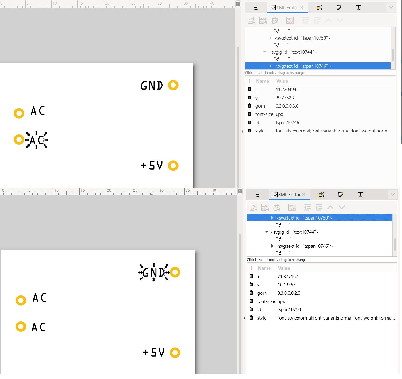
Error 69: File
‘svg.schematic.EasyPower_SO5V1000_926589be4af404b0a68a8a53c88a64f9_2_schematic.svg.bak’
At line 27
Found a drawing element before a layerId (or no layerId)
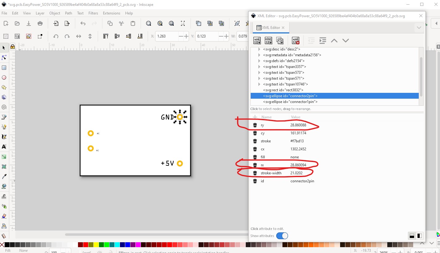
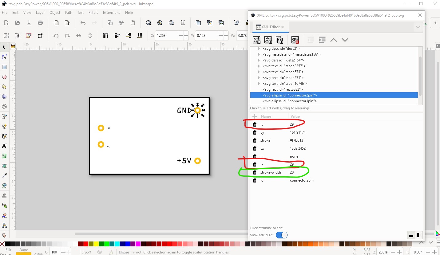
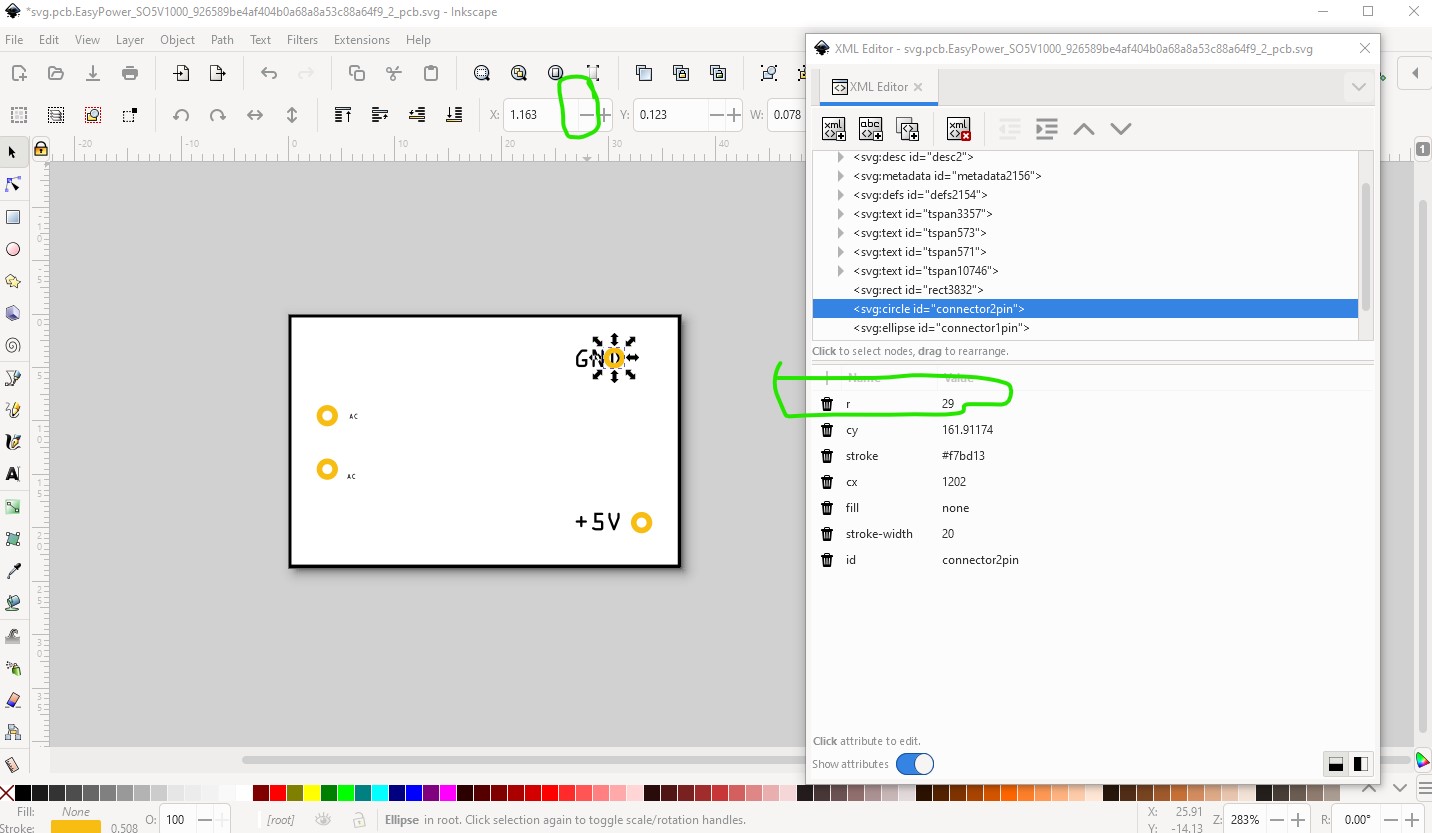
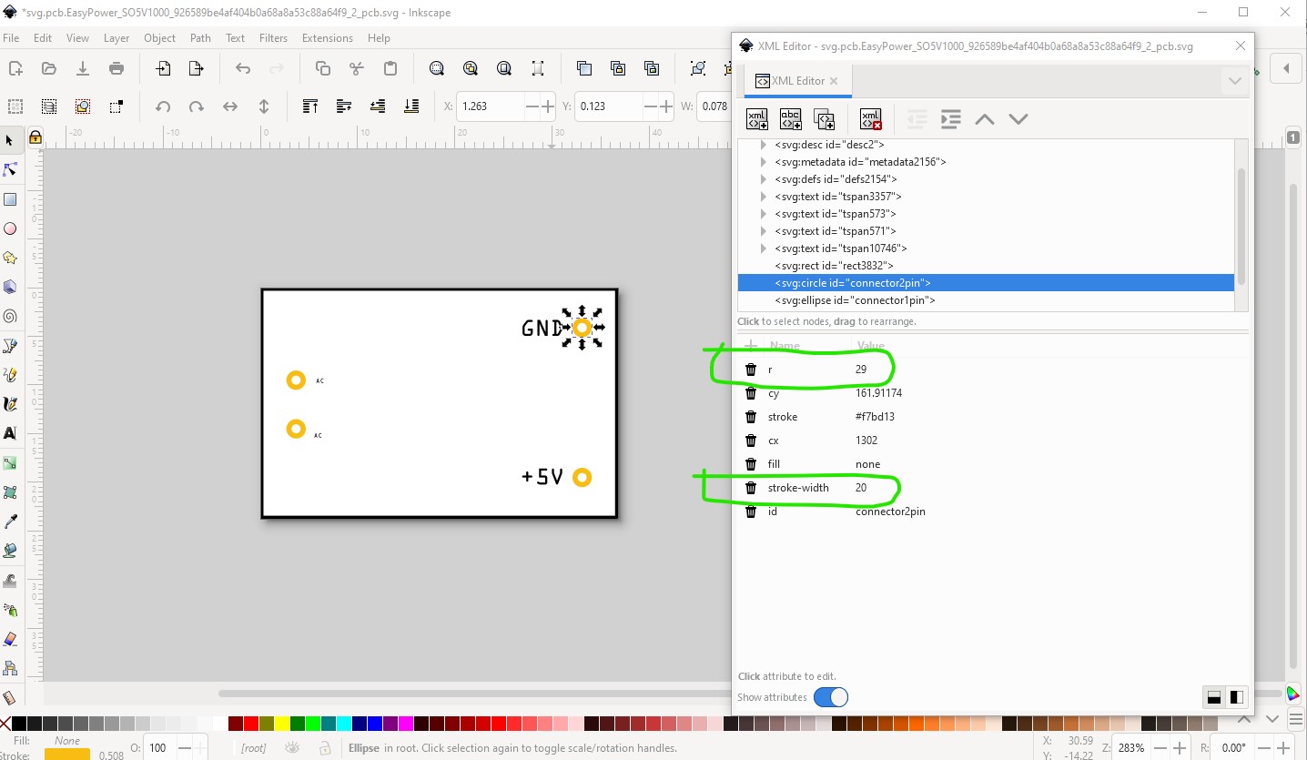
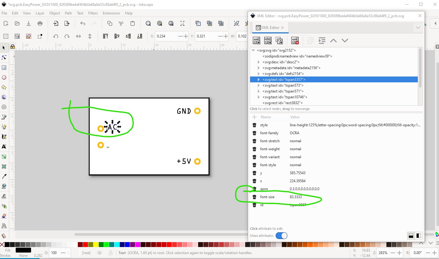
Error 65: File
‘svg.pcb.EasyPower_SO5V1000_926589be4af404b0a68a8a53c88a64f9_2_pcb.svg.bak’
At line 52
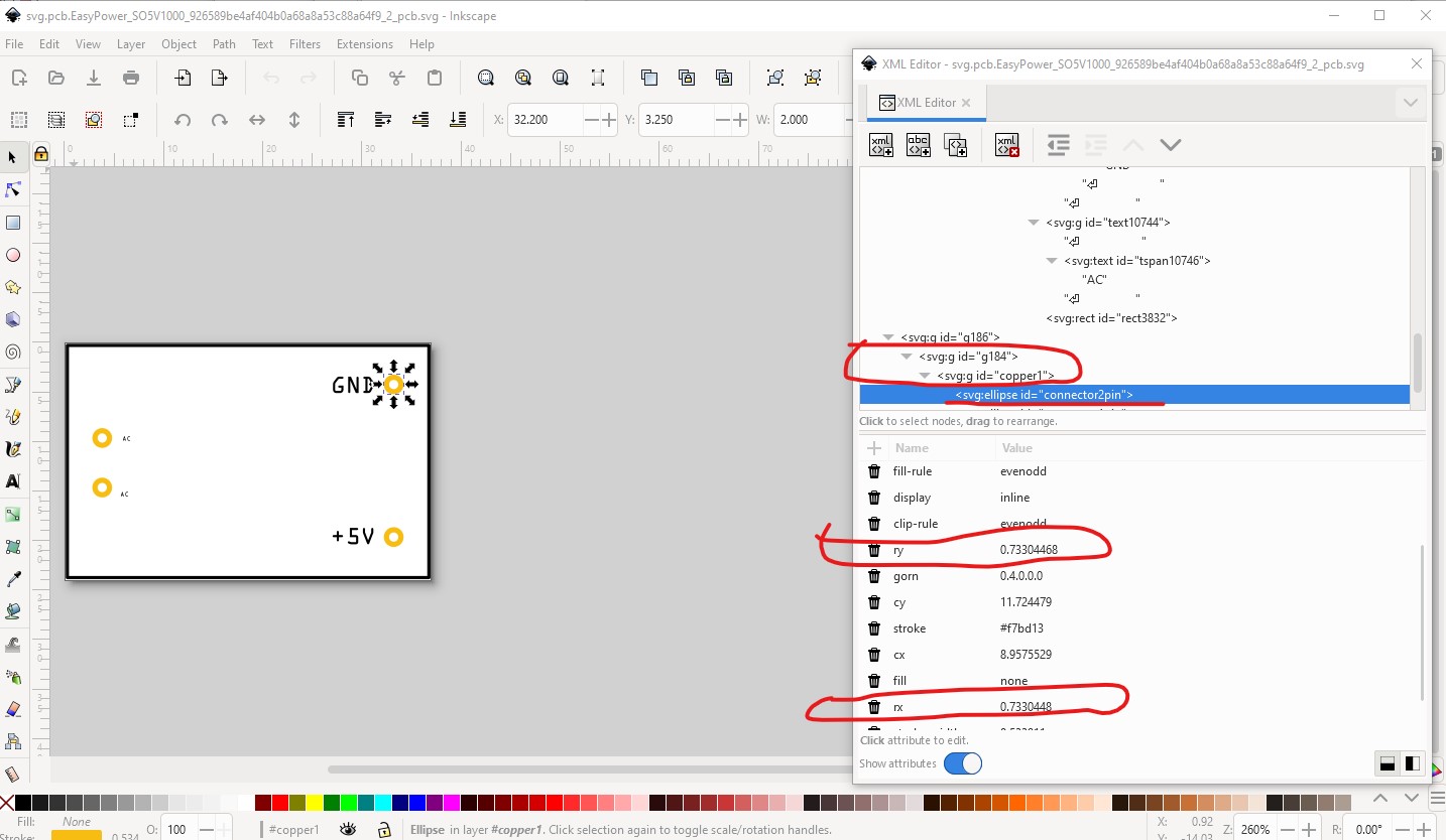
Connector connector2pin is an ellipse not a circle, (gerber generation will break.)
Error 74: File
‘svg.pcb.EasyPower_SO5V1000_926589be4af404b0a68a8a53c88a64f9_2_pcb.svg.bak’
At line 52
Connector connector2pin has no radius no hole will be generated
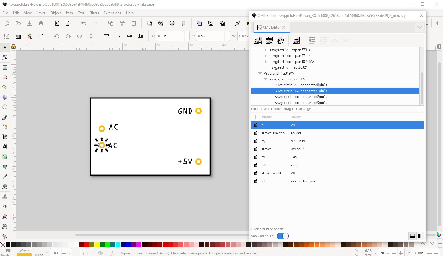
Error 65: File
‘svg.pcb.EasyPower_SO5V1000_926589be4af404b0a68a8a53c88a64f9_2_pcb.svg.bak’
At line 53
Connector connector1pin is an ellipse not a circle, (gerber generation will break.)
Error 74: File
‘svg.pcb.EasyPower_SO5V1000_926589be4af404b0a68a8a53c88a64f9_2_pcb.svg.bak’
At line 53
Connector connector1pin has no radius no hole will be generated
Error 65: File
‘svg.pcb.EasyPower_SO5V1000_926589be4af404b0a68a8a53c88a64f9_2_pcb.svg.bak’
At line 54
Connector connector3pin is an ellipse not a circle, (gerber generation will break.)
Error 74: File
‘svg.pcb.EasyPower_SO5V1000_926589be4af404b0a68a8a53c88a64f9_2_pcb.svg.bak’
At line 54
Connector connector3pin has no radius no hole will be generated
Error 65: File
‘svg.pcb.EasyPower_SO5V1000_926589be4af404b0a68a8a53c88a64f9_2_pcb.svg.bak’
At line 55
Connector connector0pin is an ellipse not a circle, (gerber generation will break.)
Error 74: File
‘svg.pcb.EasyPower_SO5V1000_926589be4af404b0a68a8a53c88a64f9_2_pcb.svg.bak’
At line 55
Connector connector0pin has no radius no hole will be generated
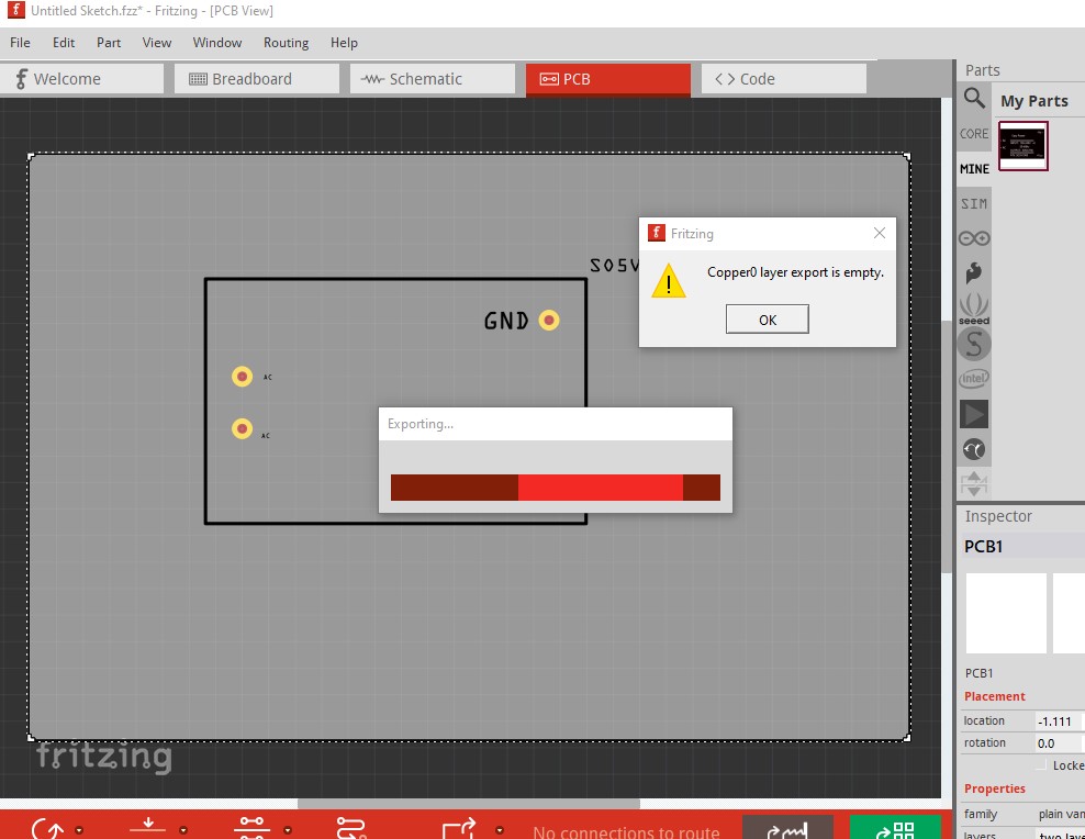
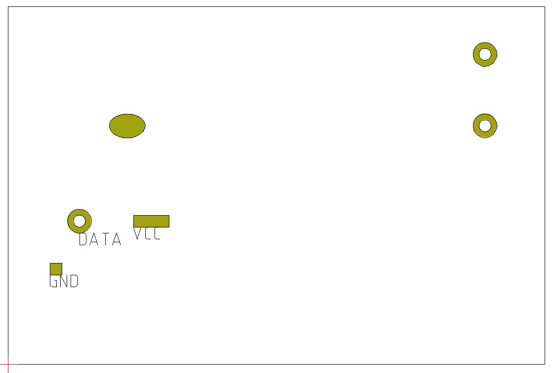
The no radius errors are because the pcb svg is incorrect and thus won’t (and doesn’t) create proper gerber files.
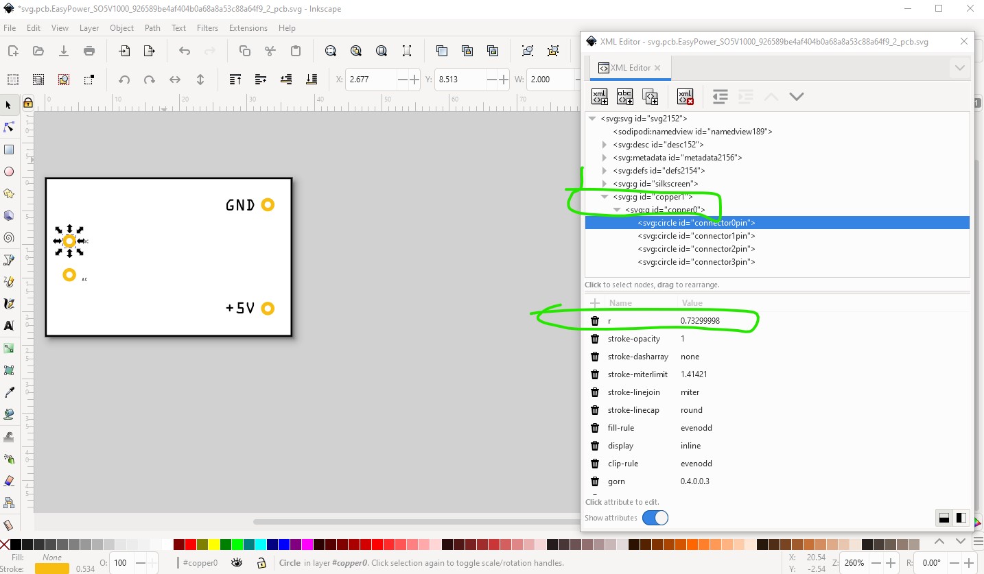
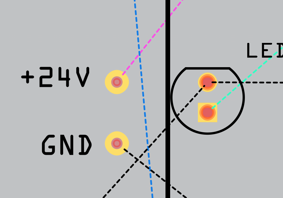
This is because the pcb svg needs to have a copper0 group as a child of the copper1 group and the pads need to be circles not ellipses as they currently are:
needs to change to look like this:
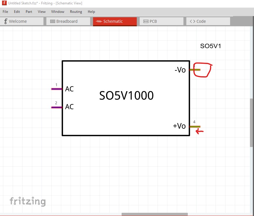
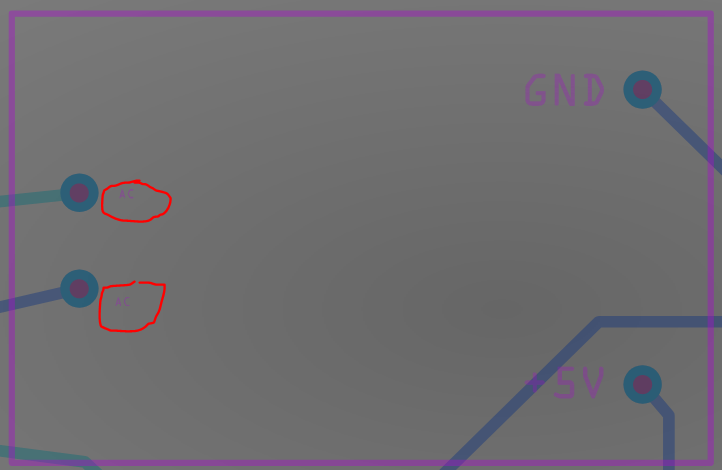
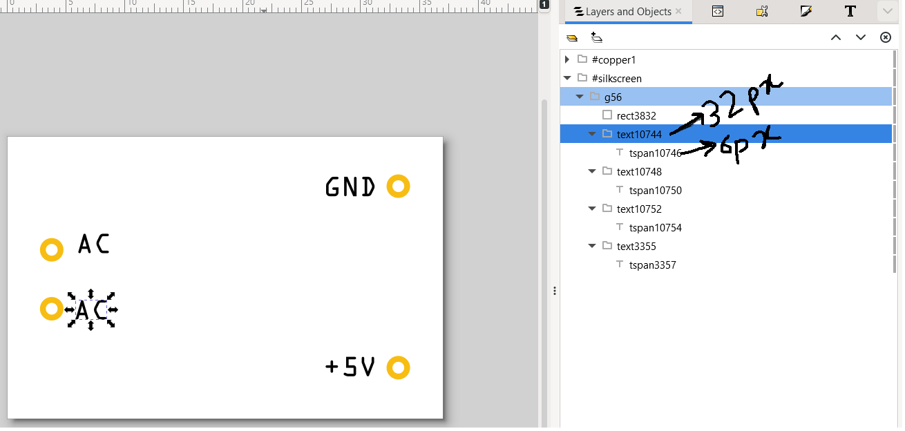
all the silkscreen elements are in a group labeled silkscreen (which needs to match the layerId in the fzp file) and the connectors are circles in group copper1 which contains group copper0 which contains the pads. This will export correctly to the gerber output to make boards. You also need to set the hole size to an appropriate value (the data sheet for this part doesn’t have enough information to tell what the hole size should be, so I would default to 0.038in which is the size to take a 0.1 header pin. With the current pcb svg you can only route traces on the top of the board (because only copper1 is defined.) Schematic you would be better to run Randy’s Inkscape extension because it will do this correctly automatically, but your current schematic is not correctly aligned to the grid:
The two pins circled in red need to move back a bit to align to the 0.1in grid lines. There are also standards for the color of the text (which the extension obeys.) Making correct parts is without a doubt complex, but to successfully make parts you need to understand all the things that need to be done. As well it is not correct that you can’t make parts from scratch, I do it regularly. That limitation is because parts editor was not finished when development stopped and parts editor has limitations on what can be changed (for instance you can not change the number of pins defined in the fzp file in parts editor AFAIK.) That is where the requirement that you start from an existing part (which is a good idea anyway even if you know what you are doing as it is less work!) comes from. If you don’t use the parts editor (which I normally do not) that isn’t a problem. The warning about missing layerId means the part will not be exported as an image (svg, jpg etc.)
Peter