Hi,
I found 3 open circuits in the manufactured boards, but the fritzing files looked ok. I submitted a complaint to the pcb factory but Can you please check as well?
Here is my complaint to the pcb factory:
"Hi, I found 3 open circuits:
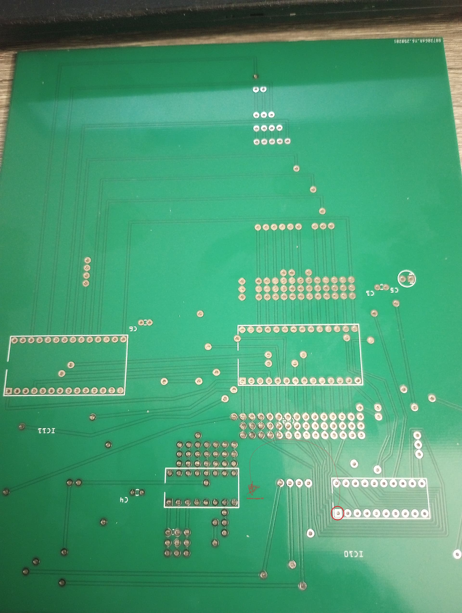
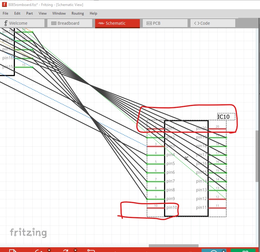
IC10 Pin 20 ↔ top layer copper fill, should be connected, see IC10_a.jpg, attached
IC10 Pin 1 ↔ bottom layer copper fill, should be connected, see IC10_b.jpg, attached
IC2 Pin 14 ↔ bottom layer copper fill, should be connected, see IC2.jpg, attached
there are connections on one layer or the other (and the holes are likely plated through) so this should be fine. There isn’t sufficient clearance on the bottom layer for the connection or it optimized the connection on one layer away (I don’t know which) but either way it will be connected via the plated through hole. Have you checked connectivity on the board with an ohmmeter? From the gerbers I have it should work. If you are on an older Fritzing version there may be bugs (gerber processing had a number that have been fixed.)
I am on v1.04. I had checked both sides even though it is plated through and only one side sufficed to check with a continuity checker. Yes, I used auto-routing on part of it, rest-manual routing. I also checked the gerber output online at jlpcb, but their viewer isn’t that great, so I was only able to verify that the top layer was good. I will wait for their reply and see what happens…
Does this mean that one side or the other lacks continuity? That would indicate a plating through error as the top pad doesn’t connect to the bottom pad. With plated through holes I would expect the board to be fine.
I expect the reply will be that the board matches the gerbers that you provided.
I hope not and they send me new boards. Just communicating with their customer service who screens complaints before going to the engineer, is a “Challenge”.
I am still unclear on what the problem is. Do the pins you specified not have continuity to the ground plane? From the gerbers (assuming plated through holes that connect) they should. As noted if the top pad doesn’t connect the the bottom pad there is a plated through error (which is a manufacturing problem and I think quite rare.) If there is no connection to the ground plane there is likely something wrong in the gerbers and new boards won’t help, although my gebers don’t indicate that. A continuity test of an actual board is going to be the best bet and I doubt the manufacturer has a board any more.
Just 3 open circuits, via to top copper fill ( for Vcc connections), 2 vias to bottom copper fill(for Gnd connections). I was only checking with you in case I did something wrong. I tested 2 whole boards completely.
Do the pads on the top connect to the same pad on the bottom? If not there is a plated through error. If the pads connect but the traces don’t there is likely a gerber error (although it isn’t showing up for me) and a gerber error is a Fritzing problem and new boards likely won’t help which is why this is important. You need to know where the problem is to determine if the problem is yours or theirs.
Thanks, Peter, the pads on the top and bottom are connected for the 3 open circuits, so I am fine in this regard. I also checked some other random pads for each IC and it worked as well.
Additionally, I was able to verify that the Gerber Output on their server is consistent with our output for the 3 open circuits,
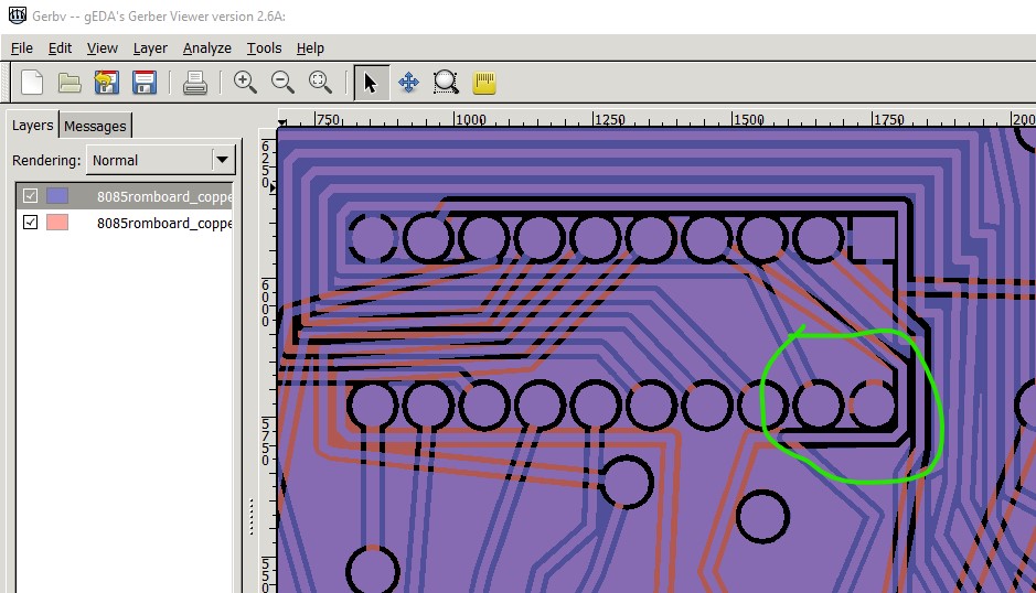
If the plating through isn’t the problem, then there appears to be a gerber error and thus new boards won’t help until you figure out the gerber error. There is in fact a gerber error, the gerbers show no connection to ground on pin 1 of IC 10. We need to figure out why that is and correct it. They likely made the boards correctly the error is on Fritzings part.
I’ll take a look at the sketch and see what I can see.
edit
You can recover the boards by using jumper wires (I typically do this with 30 ga wire wrap wire) to connect the unconnected pins to ground. Looks messy but saves the cost of replacement boards.
edit2:
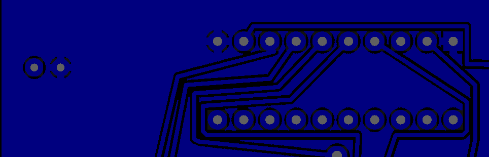
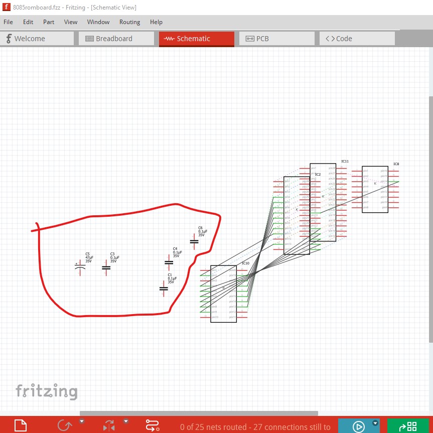
Your sketch is wrong. This is why routing schematic is always a good idea. It would have shown you are missing needed connections. There is no connections to any of the capacitors
nor any connections to the ground and power pins of the ICs which will make the board wrong (and ground fill to fail as there is nothing in the ground net.)
I see no indication of IC types, but usually there will be ground on pin 10 and power on pin 20 for most ICs (some are different) and there are no connections here to any power source so this won’t work nor will the ground fill because there is no ground net. None of the capacitors (which are likely for power supply bypass) connect to anything.
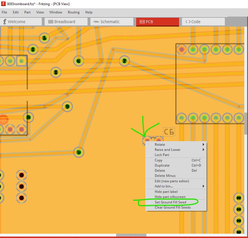
Hi Peter, I thought that power and gnd and other connections can be connected to the copper fill if you set them as ground seeds, my other vias work this way and all my capacitors and other vcc/gnd connections work fine, why just these three don’t work, did they get “unset” as ground fill seeds"?
I do this so the routing is less complicated. Its worked on other boards too, so while they appear unconnected, they are.
Then I solder header pins to vcc and ground of one ic, and the whole circuit gets powered.
I am ok with wirewrapping the 20 pin ic, but for the other ic 28 pin zif sockets don’t come in wirewrap form, I guess i can stick a wire in the zif along with the ic.
You shouldn’t need wirewrap sockets, either IC pins or standard sockets (or ZIP sockets) should do, the purpose of wire wrap wire is it is 30 gauge (although somewhat hard to strip, but I have special wire wrap strippers) and thus easier to wrap around either socket pins or IC leads to make needed connections on the pcb. If you don’t mind cutting new boards routing schematic and adding the appropriate power and ground connections as needed and then using ground fill should do what you want. With connections in schematic Fritzing will have a netlist so it knows where connections should go in pcb which makes mistakes less likely.
A late thought, I suspect your problem with no fill is due to not enough clearance between the traces to give the fill a path (with the keepout values) to get a connection to the fill copper. Moving the traces around the pins with the fill to give it that space may help as maybe adding a via to give it a path to the copper fill on the other layer. I haven’t yet tried that (and I don’t know that much about fills as I don’t usually use them) but I suspect that is the answer here.
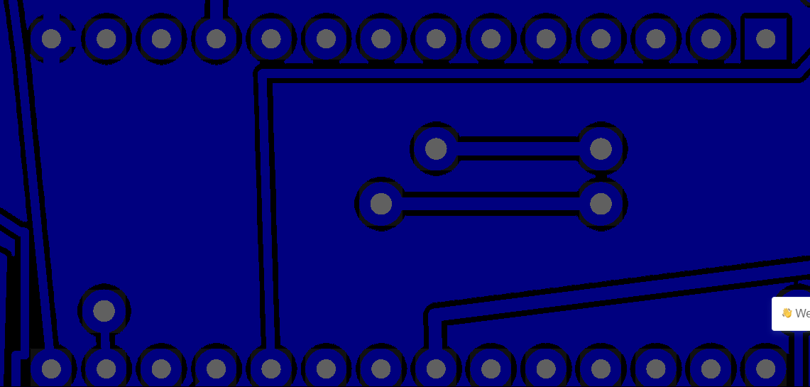
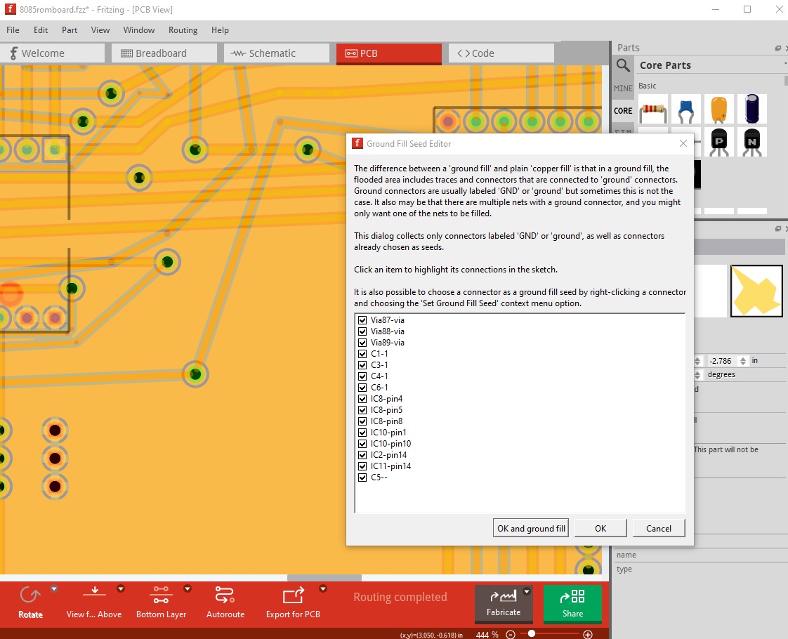
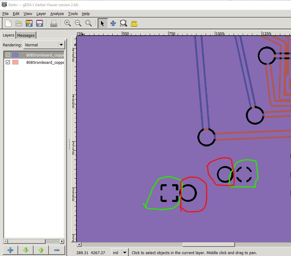
but the copper fill seeds (if they exist) are a mystery as they don’t show anywhere that I can see. The ground fill shows up when right clicking the connector
but the copper fill does not (yet the connection appears to get made!) and I don’t see how without the connector being part of a net (although as noted earlier I am not all that familiar with fills.)
so there is something I am missing here. If I can figure out how to recreate the fills correctly I can modify the sketch and try and get the fills to work correctly by giving them a path. In general Autorouting is an easy solution but it is always sub optimal (even in commercial packages costing $100K per seat) because auto routing is a vary hard problem and thus manual routing is the preferred method.
edit:
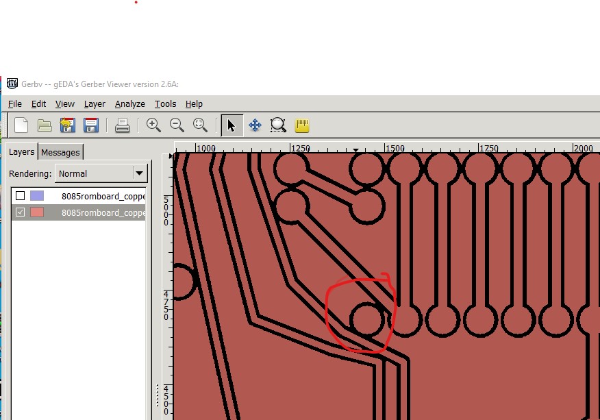
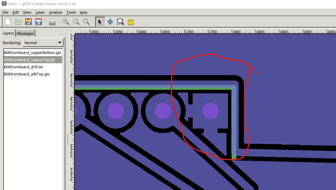
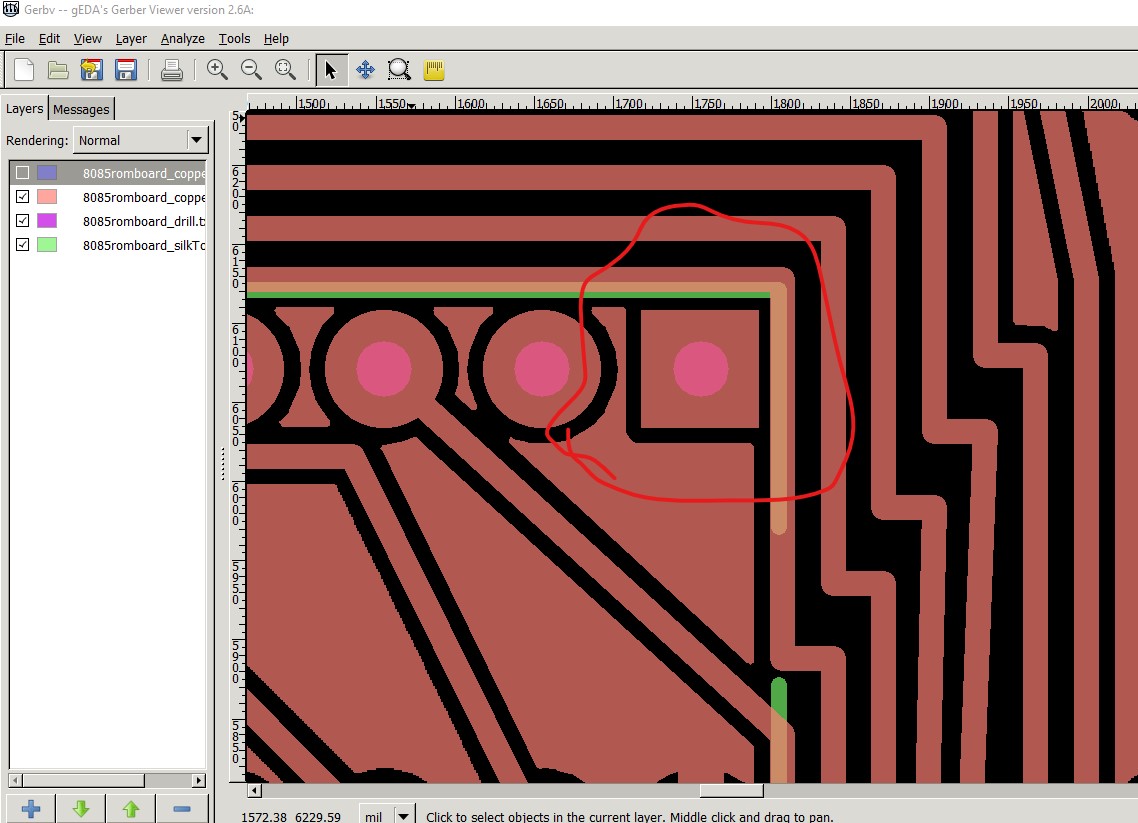
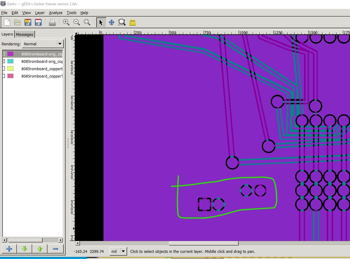
Here is what I mean. I started with your sketch then deleted the copper fill (the underlying image) then did a ground fill.
but that only does the ground fill, somehow you managed to get a copper fill for a VCC fill that I don’t get with only the ground fill and thus the output isn’t the same as yours and I can’t figure out what you did to get both fills. This is the gerbv gerber output from my ground fill.
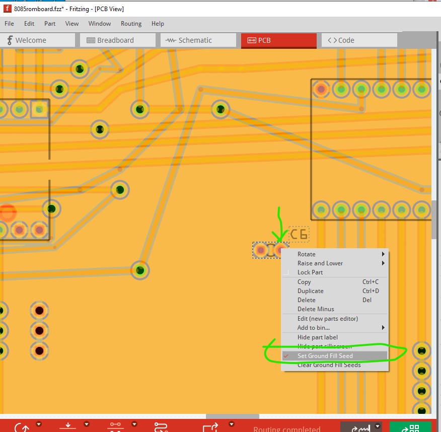
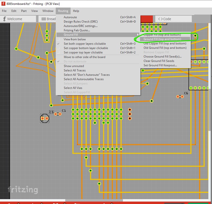
Hi Peter, I only set ground fill seeds in 1) and 3) below. I used the trick to select only the top layer prior to top layer ground fill and only the bottom layer for bottom layer ground fill.
Use top layer for Vcc Net & fill, create ground fill.
Clear the seeds
Use bottom layer for Gnd Net & Fill, create ground fill.