Hello.
It probably exists already but I can’t find it. I’m looking for an exploded view of an arduino in Fritzing format. Ideally a Mega 2560 Pro, as said in the title.
The idea is to have ON THE SAME PCB a full Mega 2560 Pro Mini and the other CMS electronic components I need. I will of course delete all the pinholes, to keep only the links I need.
I’m a developper, not an electronic ingeneer, so creating it from a white page would be a bit tricky for me, despite there are not so many components…
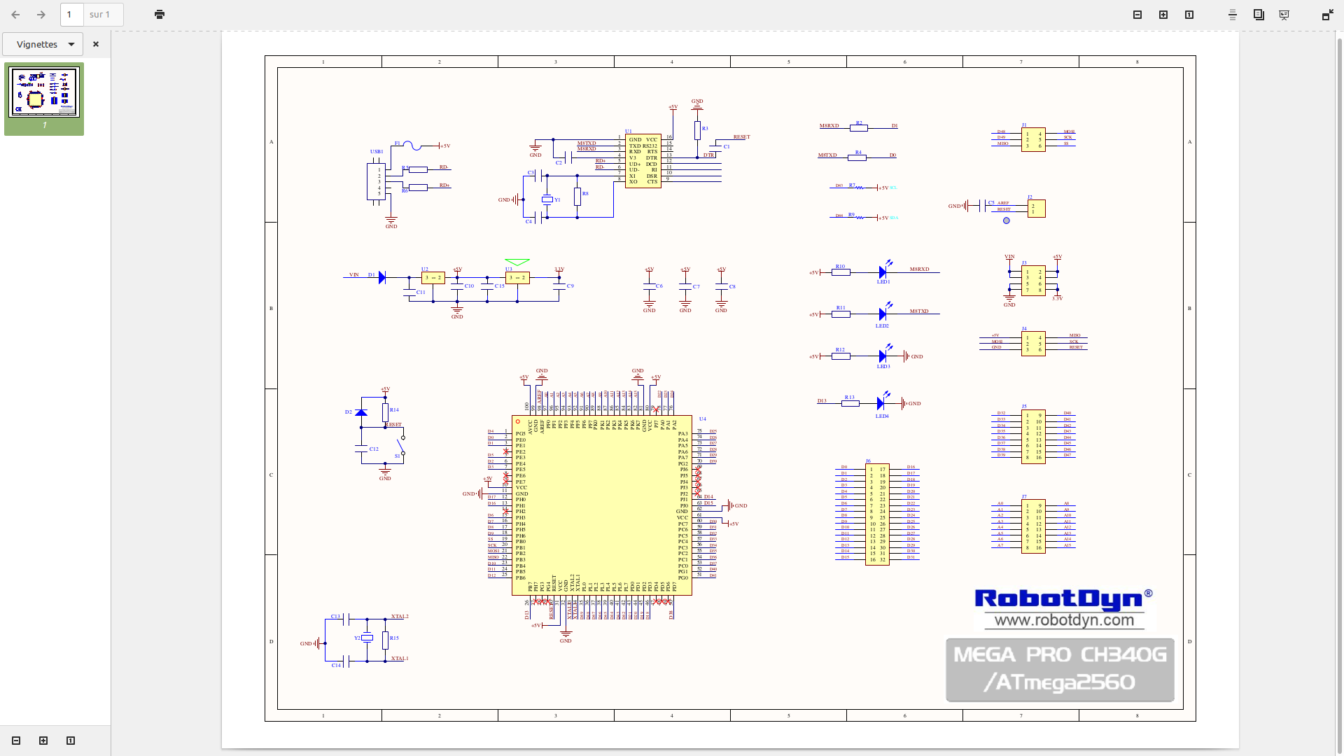
Your description of what you want is unclear. You are talking about PCB, but the image you show is schematic. You also mention deleting pin holes.
My guess is that you want to create a project with a ATmega2560 chip, but not using an Arduino board. So you want the circuit and layout of the Mega board, to be able to add your own components to it.
I am not aware of project or part file for an Arduino board with the level of detail. However a web search for “fritzing ATmega2560 circuit” turned up Creating a standalone atmega2560 5th down on the list. That has someone else’s version of what I think you are doing, with links to related things. Be careful if using that directly, as the thread comments say there are some errors.
You need to be clear about what you are intending to do. When the scope seems to broad, it is hard to answer, and can get ignored.
" My guess is that you want to create a project with a ATmega2560 chip, but not using an Arduino board. So you want the circuit and layout of the Mega board, to be able to add your own components to it."
–> You understood my needs. More preciselly, I don’t need the layout (=the distances between each component). The schematic (with correct components values) and correcponding circuit would be enough.
I already know the page you mention (thank you for your search!) and I’m already working on it. The problem is that he started under fritzing but then moved to Eagle. Another person (Eadan) gives some clue of the requiered changes,so I think it should be possible to adapt. But I would have prefered to start from a “confirmed” Fritzing file, because I’m a developper, not an electronic engeneer, so if my board does not work because of an uncorrect component I won’t be able to identify the problem…
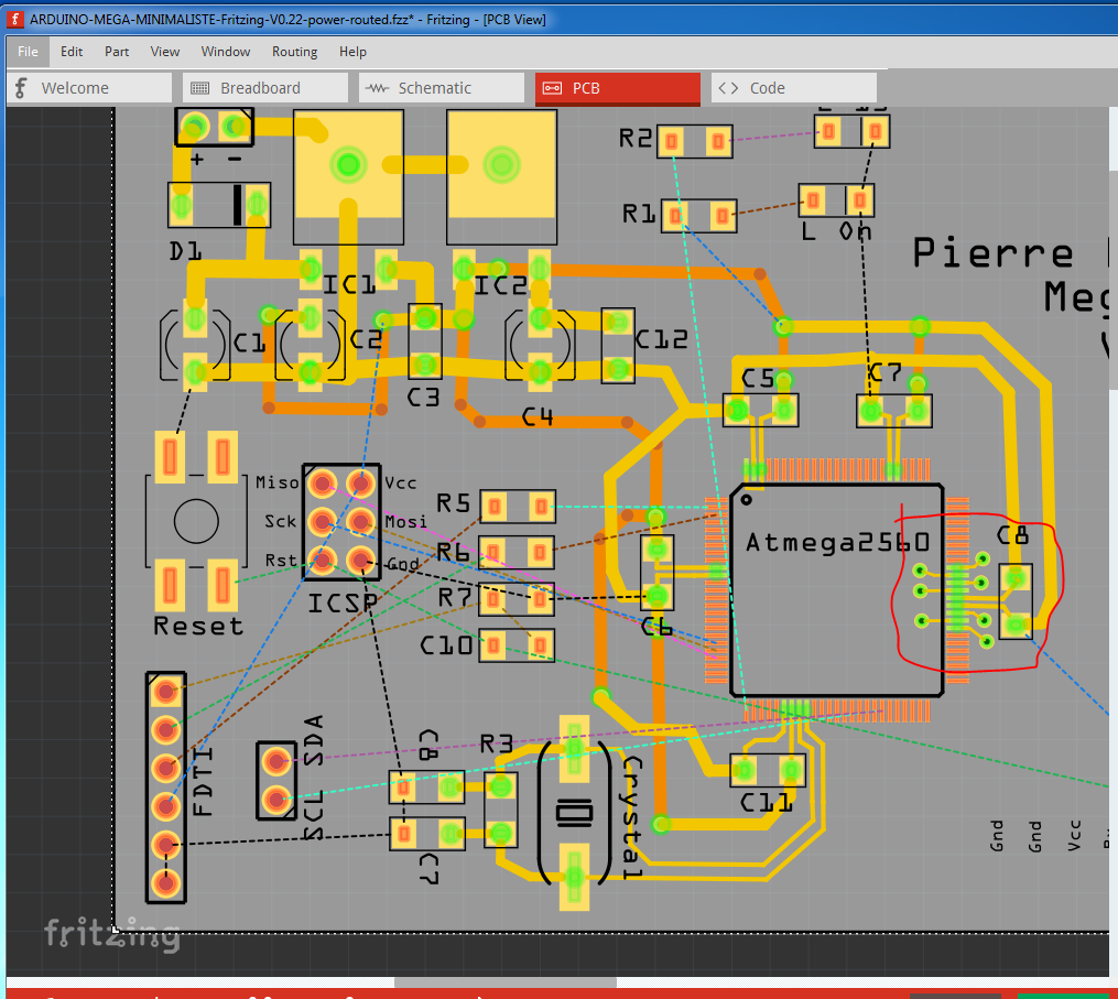
This is what I got so far, using SMD components only. But I still have some problem, like the fact that Fritzing does not offer 22pF capacitor. So I put 10pF instead but I don’t know if it is correct.
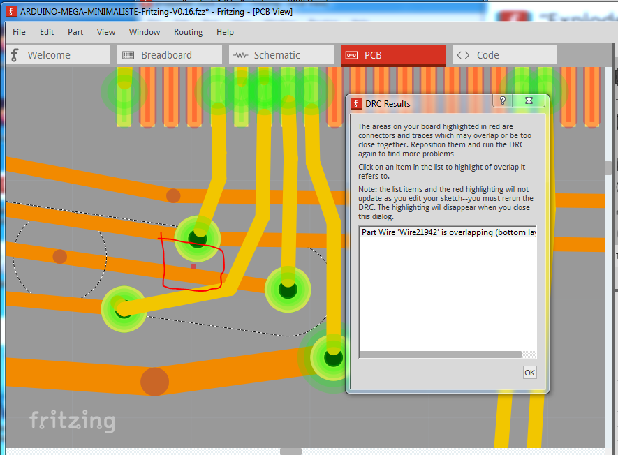
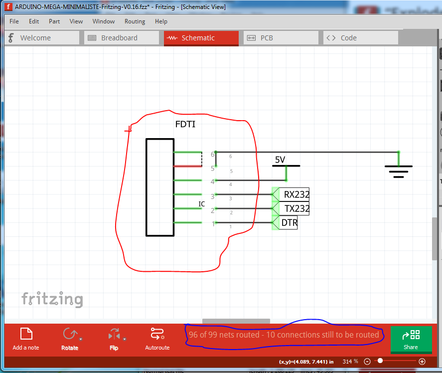
so you need to move the traces so there is more room between them. In schematic the fdti part has some connection problems and there are a number of nets not connected properly:
All wires are more distant than 0.19mm, but none of the wires linked to the Atmega respect the advised 0.24mm distance, except if I reduce the wires width to their minimum (8mil), which seems very, very narow. Would you recommand to leave as is or reduce the wires width?
As long as the traces meet the minimums of the board house you should be fine as is. The first time I looked at this I was looking for Fritzing problems, this time I see a couple of design related issues. The crystal is way too far away from the CPU. It needs to be as close as possible with short leads not a long way across the board with long leads and vias. The same is true for the bypass capacitors for the CPU, they need to be as close as possible to the power and ground pins on the CPU, not in a row by the voltage regulators. From the extra (unconnected) chips I expect there is more to come on the board. You would be best make all the connections you want and then move stuff around to make the connections as short as possible (and to make sure you have enough space for the components and traces on the board!) You likely also need a power on reset circuit (a capacitor and resistor on the reset circuit to keep reset low until power is stabilized) which isn’t currently present.
I wanted to design a generic board, so that it could be helpfull to other people, but you are right: if I need to move all these capacitors closer to the microcontroler, I should then add my other components right now, so that I can access all the pins needed. I finish my PCB and send it here
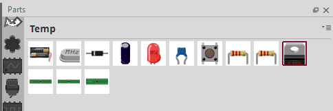
All the capacitors except c7 and c8 (on the crystal) and c10 (in the reset circuit) are bypass capacitors. On the CPU chip you want bypass caps (typically .1 uf ceramics) as close as possible to each vcc and ground connection. You will also need sufficient space to get traces out from the CPU chip for all the I/O lines and I don’t think there is currently sufficient space to do that. As well your sketch has a bunch of standard core parts in the temp parts bin, indicating that the parts have been modified in some way. Why not use the core part versions?
I understand that the cristal and bypass capacitors should be as close as possible from the microcontroler, but are you shure it must be that close? Because when I look at a standard board they are more than 1cm away from the microcontroller (except 2 of them)…
That would be a good bet. That said I’m curious why you need adapted parts for resistors and capacitors though, they are standard parts.
Unfortunately no, there are two types of bypass capacitors and C1 C2 and C4 need to be 10uf for the regulators to supply peak currents. The .1uf capacitors are to eliminate high speed noise (which the 10uf caps won’t.)
Usually not a good idea. You want a higher voltage than the supply for the capacitors usually.
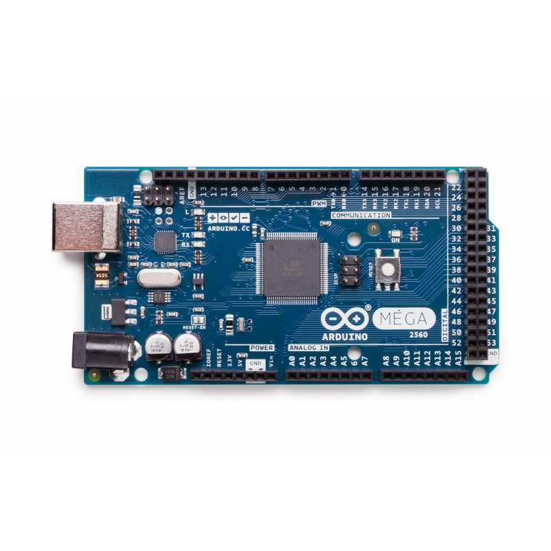
You want at least as many (it looks like 3 from the photo of the mega) as the arduino folks used (although you need to check the bottom of the mega board for more bypass caps that don’t show in the top photo!)
It looks from the photo that it indeed doesn’t need to be that close. I expect the routing still wants to be as direct as possible. At worst the CPU won’t work when the boards are made which means you will have to redo the boards. Can the components all be moved around to simplify the routing? Is there any thing that needs to be where it is on the board for external reasons? If not, when you have cleaned up the temp directory I’ll have a look at routing the board in minimal space.
edit:
I think you may have routing database problems, some of the rats nest lines in pcb are acting strange. That said here is a sketch with what I think are the correct bypass caps (I added 2 .1uf caps, one for the 3.3V regulator and one for the atmega.) As you will see I removed all traces and all vias (and the text) to start from scratch. As well I moved things around to make routing easier and the distance to the crystal shorter while hopefully leaving room to run the power connections. I’m assuming here that there are no physical constraints on the board (i.e components can be moved to simplify routing.). The power and ground runs from the regulator still need to be routed, but this is a likely safe bypass cap layout for both the regulators and the cpu.
The main change (other than more traces) is to route the power mostly on the top layer, leaving the bottom layer (and a lot of vias!) to route the I/O pins of the CPU. I did the I/O lines around C8 in this image (circled in red here) as an example. You will need to have room for vias for pretty much all the I/O pins (but most of the bottom layer is then available for routing them too!)
I routed this with snap to grid off, so for the real thing you would need to set an appropriate grid size and enable snap to grid to align the traces correctly.
edit: One late thought: you need to check the footprint for the electrolytic capacitors. The one in Fritizng are generic and the actual capacitors you intend to use may not be the same footprint as is in Fritzing! So you need to verify the footprint before doing the routing.
I left the old project, with a Pro Mega 2560, to help you understand
I’ve got a bug between ground and Vcc (probably an uncorrect wire somewhere…)
some wires are still crossing, it’s still messy and complicated, too many vias, sharp angles, wires too close and temp components not deleted (I’ll correct it later)
I deleted the 5v converter to spare space, as I don’t need it–> Did I do it the right way?
The joystick, screen and pulse are in their final position, everything else can be moved if needed
I volontarily did not put capacitors around the joystick, to spare space: the debounce is managed by the software.