Yes it looks like it is fine. An issue is going to be heat in the regulator though. Depending on how much current this draws, the regulator may over heat as it will be dissipating around 4W assuming a current draw of 500ma. It would be a good bet to test this by breadboarding the 3.3V regulator driving a 3.3V Atmega board from 12V. You may need to use a buck regulator module to get from 12V down to 3.3 with minimal heat.
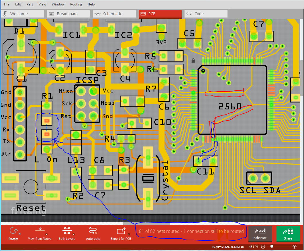
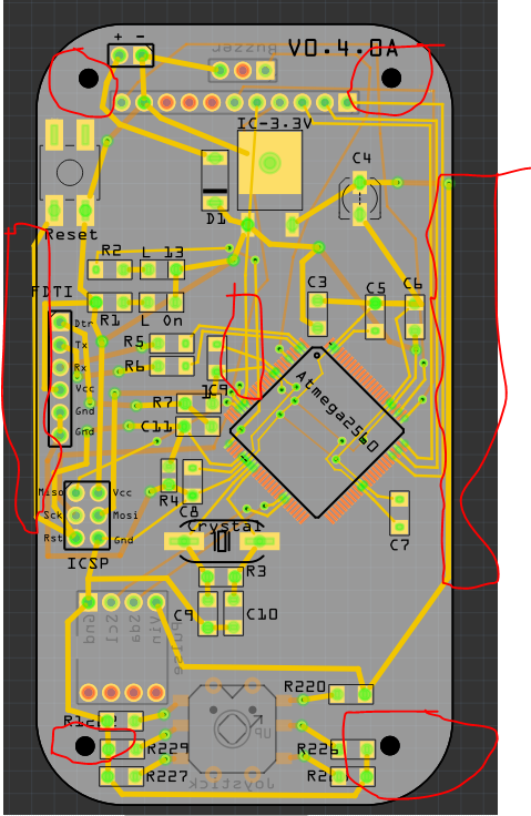
The traces outined in red on the edge of the board are too close to the board edge. The components and traces around the mounting holes are likely to close to the mounting holes and will interfere with the scews. As you note there are a bunch of overlapping traces and a power to ground short somewhere.
For your other board, I made a new part for the FTDI board, you may want to use that here as well. If you want to make modified parts you would be better to learn to make custom parts (which is not easy) rather than using the IC and renaming pins. There are currently bugs in that code which are showing up in your schematic.
I am still poking at your original board, I have it fully routed but need to clear the routing database corruption. Once I finish that it may give you an example of how to remove some of the vias.
OK, here is your original board fixed up. It turns out the routing problems are a bad part: the atmega chip in core is missing the power and ground bus definitions which cause the routing errors. There is a partially fixed (there are still some issues in the svg files that don’t affect part operation that I need to fix later.) cpu in the temp parts bin here. The board passes DRC and is about 1/2in less tall than your original. C1 needs to be a 605 case not 405. The 90 or so vias are to insure that every I/O pin on the cpu can in some manner (mostly on the bottom layer) make it out to the rest of the board. The 3.3V regulator output will need to go back to the left to get out to the rest of the board, but there is a path there to do it. I moved the reset switch to the bottom left of the board for easiest access. The grid size is currently set at 0.25mm (half the IC pitch), which seems to be working well enough. I changed the version number to 2.3 as well. Hopefully you will make a board from it and we will see if it works . I expect it will be useful to others that want to make something based on the mega cpu.
Thanks a lot, vanepp, for all the time you spent on this project. Your board is impressive. And you saved so much space! Let’s hope it will be usefull for many people!
→ Interesting. What did you change?
Don’t all the VCC and GND pins of the microcontroler need to be linked? I thought they had to (the datasheet of the Atmega2560 does not mention if they are already linked inside the chip or not).
First someone needs to build one so we know if it works or not .
Yes they all need to connect on the micro (and I expect they are not linked internally), but this was internal to Fritzing. In the part, in schematic all the power and ground pins are overlaid on a single pin (which is fine), but for routing to work properly the pins all need to be part of a bus so a connection to any pin is a connection to all of them. The bus definition is missing from the part, and that causes the routing issues. The svg files need some style clean up and then I’ll submit an update for core parts.
No need to wait for the update, the part in the temp bin works fine. The svg changes are all style not functional, they won’t affect the operation of the part.
Slight corrections:
-one of the leds was upside-down
-I deleted the vias of the unused pins of the controler
-I linked the microcontroler VCC pins
-I moved outside the microcontroler area as many vias as possible
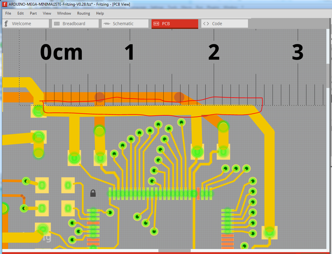
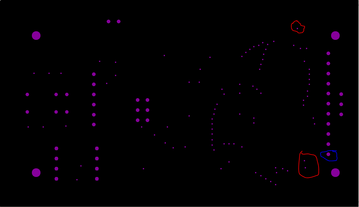
A few corrections in turn (this is why peer review of board design is aways a good idea!) There is a trace missing, and the CPU power connections short reset to VCC (off by one pin) and produce ground loops (where one pin has 2 or more parallel connections to another pin.) This is your 0.28 version with the problems circled:
The “one net to route message” (circled in blue at the bottom of the window) is because of the missing trace between R1 and the ON LED. The red/blue circled trace on the CPU is off by one, and shorts Reset to VCC. The two red circled traces cause a VCC ground loop where there are two different current paths to the same pin. This can be a problem (especially on power and ground) when high current causes a voltage drop across the traces. With two paths, current will flow in the higher resistance path to the lower voltage which is very undesirable. All connections should only have a single path to any other pin (no parallel connections.) Once those were corrected, I cleaned up the routing to meet best practices. Best practice is that connections to a pad should be at right angles, and intersections in traces should be at 45 degrees (which is really most important at rf frequencies, but always doing it is the best practice, plus it reduces EMI if that is important to you.) or at 90 degrees for a straight run. Since this is a reference design it is desirable that it meet best practices to serve as an example. In addition I increased the trace size of all the power pins in to the CPU from 8mil to 12mil (the same size as the trace to the pins.) That provides a bit more current carrying capacity at no particular cost. It may be an idea to create a ground fill on the top of the board. That would increase (greatly!) the copper available to heat sink the regulators with the only cost being the hassle of adding the ground fill.
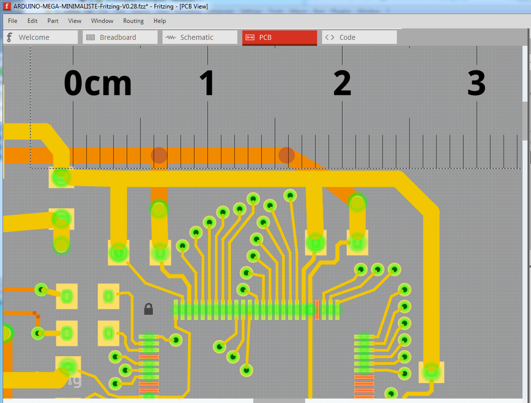
This snippet indicates the correct way (the top and bottom pads outlined in blue) and the wrong way, (the middle pad entering at 45 degrees.) Because of the fine grid size (0.25mm) insuring that the traces are straight is a challenge. The ruler in core parts provides a convenient way to achieve straightness (at least as much as we can!):
clicking and dragging it a bit straightens it up to exactly horizontal. Here is a version 0.29 of the board with these changes made (and hopefully no errors added .)
One final suggestion, what may make a good reference design is to add 1.27mm pitch (0.05in, half the size of standard .1in headers) for all the I/O pins to make a complete ATmega mini board with the I/O pins out to headers just like a full size ATmega. The down side to the 1.27mm headers is that there are no (that I know of) patch cables for them. I made some (because I have wireless modules with 1.27mm connectors) out of a bunch of single pin milmax single pin solder connectors (with the other end being a standard .1 header connector) but they are $2 Canadian each (when I bought 25 the first time they were $1 ea at mouser, but they now match digikey at $2 ea!) This is the only single pin 1.27mm jack I know of though.
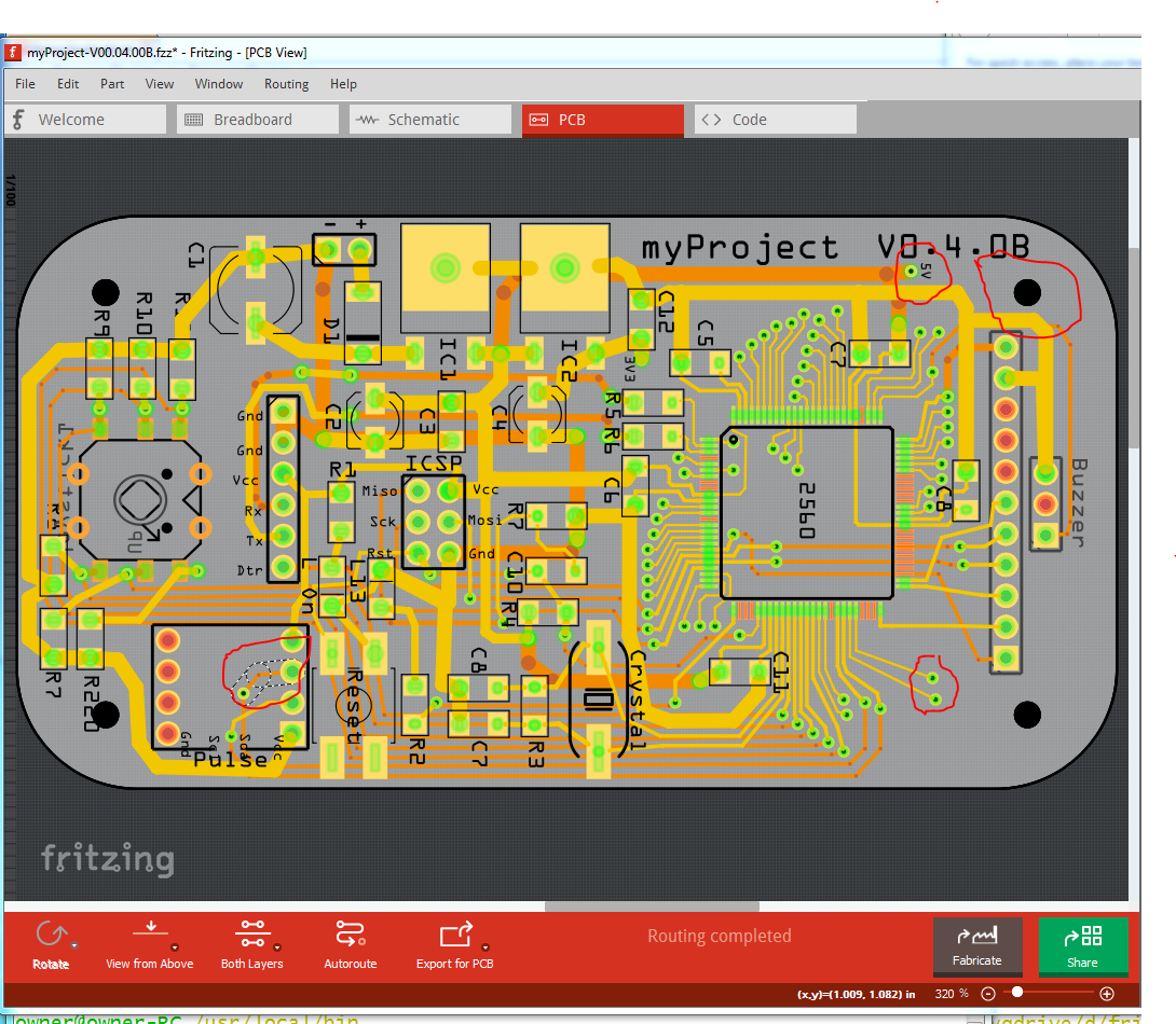
Here is the PCB of my project. Could you please have an eye on it, just in case, before I order if?
Thanks, and happy new year (a few hours in advance…)
Some informations:
-the 3.3v and 5v vias are just for the tests. They will be deleted
-I also left all the vias around the microcontroler. They are useless, of course (only for tests).
-the software has re-created parts in the Temp directory. I don’t know why. Only the screen is self-designed.
-The final project will only have a 3.3v regulator, a 8MHz cristal and no led, for power saving. But I prefer to validate the original 5v board first.
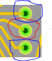
I don’t see any problems (that doesn’t mean there aren’t any, just that I don’t see them if they are there. ) A couple of minor nits that don’t affect correctness (but may affect usability and are easy to change now!) You can eliminate one via by moving the trace from the via on pulse to the bottom layer. Won’t change functionality, but one less via to potentially fail. Outlined in red in the image below (I didn’t remove the via, just moved the trace to bottom layer here.) The mounting hole on the top right is close to the VCC bus. You may need a fiber washer there to prevent shorting VCC to the case.
Last the vias on 5V and tz and rx have a very small hole diameter (0.015748in from the gerber drill.txt file) and assuming (as I am) that they are intended to take wires, you may want to increase them to 0.038in (the size for a .1 header or a wire) by either increasing the via size in inspector or replacing them with a single pin .1 header. You can see the relative hole sizes in this gerber image (from gerbv) of the holes. The vias I think are intended to take wires are circled in red, a 0.038 header pin on the near by connector is circled in blue.
With the note that I have zero experience in assembled boards, and all of my comments here are based on things I have heard in here in the past, the first issue here is likely that jlcpcb will want a pick and place file for the assembly (unless they will make one for a fee) and Fritzing can’t produce one. So I’d check with the jlcpcb folks about that first. I think there is usually a minimum order (25 boards at the pcb house I usually use) for assembly unless they have a single unit prototyping service at extra cost. As to the parts, that is more or less a crap shoot, until you build one, it is hard to say if the parts are correct. For the crystal, check the atmega data sheet for crystal specs (although I don’t see any there) otherwise look at the data sheet for the crystal you have selected to make sure the capacitor values are correct for that crystal. Note if you are running at 3.3V the max frequency looks to be 8mhz, not 16. For capacitors, check the footprint size to make sure the footprints in Fritzing are the same (or at least compatible) with the component selected. As long as the capacity, voltage and foot print match, you should be fine. Sorry I can’t be more help!
The little I know of pick and place files doesn’t sound easy , as well as the x/y coord of the part, they wanted center of gravity settings which doesn’t sound that easy. Hopefully it will work out though.
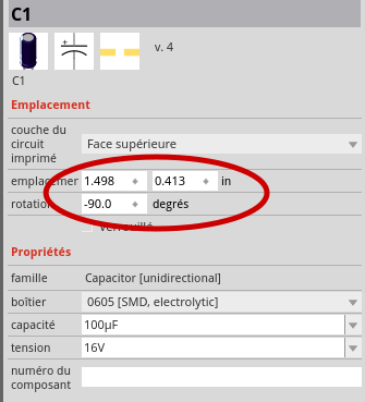
The first thing I wonder is whether the Fritzing idea of x/y is going to match the gerber output idea of x/y. Hopefully yes or your pick and place file won’t work. You need to try and figure out the gerber x y coords of a component from the drill.txt file or maybe better yet the silk_top.gto file (which appears to be in text format) and see if that matches your place file x y values! If that is all they need, then this could be fairly easily automated outside of Fritzing via a python script. First though, if you click on the “in” at the end of the circled line it will change to mm or px (which is what the xml uses.) which has been done in the image above. Using this single capacitor as an example and saving it as a .fz file:
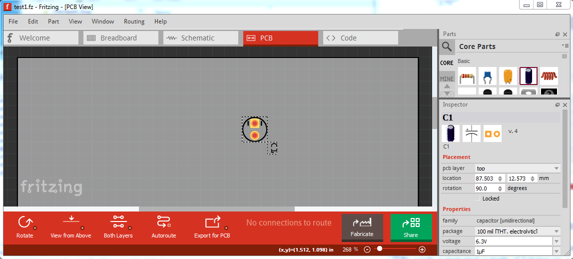
I don’t know what the Z value indicates, but x and y appear to be in px (and thus would need to be converted to mm, but that should be a simple multiply.) Rotation is harder, it looks like Frtizing uses a transform. Here C1 is rotated +90 and the xml changes like this:
so you would need to figure out how to apply the transform to come up with the degree value (there is obviously code in Fritzing which does that, but it may not be easy to find!) Given this is all xml, as I said this could be done in a python script external to Fritzing (which is likely to be the quickest solution.) However this may only work for this particular board house though, as I recall from a discussion a few years ago by someone that was familiar with pick and place files the standard version has center of gravity fields as well which is information Fritzing doesn’t have. In any case it will be interesting to see it this works!
Well, I must admit it won’t be as easy as I thought, as the Y is oposit in JCLPCB: Y=0 corresponds to the top line ine Fritzing and the bottom in JCLPCB. I have to convert in (Y2 = pcbHeight - Y)
The good news is that JCLPCB displays the result, so there is a mean to find the right values…
Converting the pnp.txt file through a script could be a solution but I don’t see what’s the distance unit used in this file…
You should be able to calculate that by finding the same component in Fritzing and the pnp.txt file then comparing the coord values. You may need to do two components to be sure. I assume JCLPCB is their layout program? If so that is good because you can make a small test board in both Fritzing and JCLPCB and verify the output gerbers and pnp.txt file from Fritzing match those from JCLPCB which should insure a correct board.
 . I expect it will be useful to others that want to make something based on the mega cpu.