Hello Kjell @kjellm and Peter @vanepp,
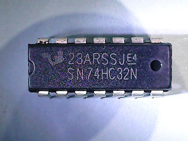
Could I please trouble you to review the attached Fritzing part, a quad OR-Gate SN74HC32N? I’m new to Fritzing, and am using an older “free” version (0.9.3b) to evaluate.
SN74HC32N Quad OR Gate.fzpz (6.1 KB)
A bit of background: I’m mentoring a high school robotics team, and the team chose to use the Raspberry Pi Pico W (WiFi) for their project. I needed a schematic/breadboard tool for the Pico, and the Raspberry Pi Foundation released a Fritzing part for it.
Our circuit(s) are relatively simple, but I needed two additional parts (a 24-pin DIP and a 14-pin DIP) not in the inventory. I used the parts editor to create the first, then took a look at the underlying .fzp and .svg files and found some strange constructs.
DIPS “usually” have only one pin 1 marker - either notch, indent, paint stripe, paint dot, etc - depending on manufacturer preferences. It appears that only a few devices show both notch and indent at the same time, and this ended up the Fritzing default. When I took a look at the actual .svg code that displayed the DIP, I found a bunch of useless-to-Fritzing tags, ID’s, and other stuff. In the case of DIP’s, there’s also very clumsy and inefficient graphics showing the chip coloration and the pin 1 notch.
Using the built-in parts editor and/or inkscape/illustrator without any subsequent text editing of the .svg’s results in duplicating all this unnecessary bloat.
I elected to hand-edit the .svg’s to clean them up.
Cleaner (smaller file size) .svg’s I think would be helpful, both from a maintenance as well as a performance standpoint. If Fritzing could deal with embedded CSS blocks within the .svg’s, that would go a long way to reducing .svg file size. Static graphics (e.g. text) would benefit from this. Pin, terminal and other connection points probably need to remain individually defined for Fritzing to be able to locate, highlight/unhighlight, etc.
The first thing I found was the breadboard units were all screwed up - still in points, not inches or millimeters. “Points” is the typesetter size unit, 72 points per inch - this is probably the standard for Illustrator, as that is their target audience. For recalculating all the DIP graphics I used AutoCAD; I subsequently used this for the schematic re-write as well. The PCB footprint was sound enough to just clean up by hand-editing the .svg.
Since inches and mils (“milliinches”) are the traditional standard in America for component size and layout, I elected to use units of inches and mils for the DIPs. I later found this was recommended in the online parts creation documentation, and strongly echo this recommendation.
The actual chips I’m using only have a notch,

so I commented out the circular depression pin 1 marker. I also cleaned up the notch and encapsulation graphics to reduce file size and modestly improve performance. I added a commented-out ink stripe and ink dot graphic, in case this .svg ends up being used as a template for other devices. I also ordered in the .svg the pin numbers in conventional order - pin0 to pin13 in this case. This actually makes hand-editing the breadboard .svg very simple as all of the repeated graphics are just 100 mils different than the previous - just one digit to change for each set of entries.
For the icon .svg, I elected to truncate the DIP illustration and only show six pins with a large 4-char text of the the meaningful portion of the device number. Simply duplicating the breadboard .svg (with all its faults) for the icon substantially reduces the usability - one 14-pin DIP with a blurry number looks like every other 14-pin DIP with a blurry number.
I added the notch graphic to the PCB silkscreen, and very slightly increased the pad outside diameter. For Fritzing, I doubt the users would attempt to sneak a trace between two adjacent pads, that’s a more advanced technique and requires knowledge of the current, copper weight, and trace width.
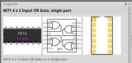
For the schematic, I elected to show the logic symbols as an aid to the students. The schematic width and height from the Fritzing part I used as a template was suitable for this. I again used AutoCAD to lay out the logic symbols, and reserved space for the “not” circle and the “exclusive” symbol, neither of which is shown on this standard “OR” chip, but results in the schematic routing within the chip outline to show jogs. It will be a trivial exercise to convert this schematic to “XOR” or “XNOR” version.
On a different forum there was a complaint that the logic symbols didn’t reflect the IEEE/IEC defined symbols. In drawing up the proper symbols as a test I found:
- If placed within the chip outline they’re much too large for the information they convey on the schematic, and
- Even the manufacturers deviate from the standard.
Sizing them down to a reasonable size slightly distorts them from the IEEE/IEC definition without affecting their symbology and conserves space on the schematic, so I chose this technique.
[ Side note: If you review the Texas Instruments datasheet for this SN74HC32N device, you can clearly see that their logic symbols deviate from the IEEE/IEC definition, as well as contain some “scrambled” graphics if you zoom in closely. ]
The older version of Fritzing I’m using doesn’t have a simulation feature, so I have not included any <spice> directives. It does look like the “copy an existing part to create a new part” paradigm might need to omit the <spice> directives. For example, it looks like the Huzzah_ESP8266 part has the <spice> directive from the Analog Devices AD8210 part. And by the way, double check the AD8210 <spice> directive - I think one of the pins is N/C so the AD8210.cir file only has seven parameters on the .subckt card.
I would think better / more enhanced part creation documentation, especially with respect to “Properties” and how they link the .fzp to the .svg’s would be beneficial. For example, I don’t think the official documentation lists some of the requirements (e.g. schematic terminal graphic) that Peter has posted separately in the forum.
Lastly, I think it would be helpful to describe (maybe with a short tutorial and an example part) a Quality Control process to confirm any newly-created part has the desired and required features. Running Python scripts can identify all the technical issues (e.g. missing pin, terminal or other ID’s) but doesn’t help locate things like swapped graphic colors (e.g. “sparkfun speaker”) or swapped terminal text (e.g. “sparkfun voltage regulator LM317”). To this end I constructed a nonsensical circuit, connecting two NPN BJT’s to each side of this DIP, and an LED across the remaining two pins. This lets me confirm that the pin/terminal ID’s are in the correct location (otherwise the BJT or LED wires cross) as well as confirm all pins and terminals are accounted for, and the PCB matches the schematic which matches the breadboard.
SN74HC32N Quad OR Gate Part Verification.fzz (12.4 KB)
TIA for your review and feedback,
- Erik -


