I have attempted to make my own part, but I do not have all the tools to make the part correctly. Therefore, could someone help with making his simple part?
The part is an ExpressLRS receiver that is made by HappyModel which is called an ELRS EP2 Receiver.
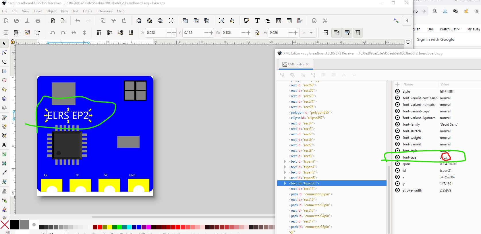
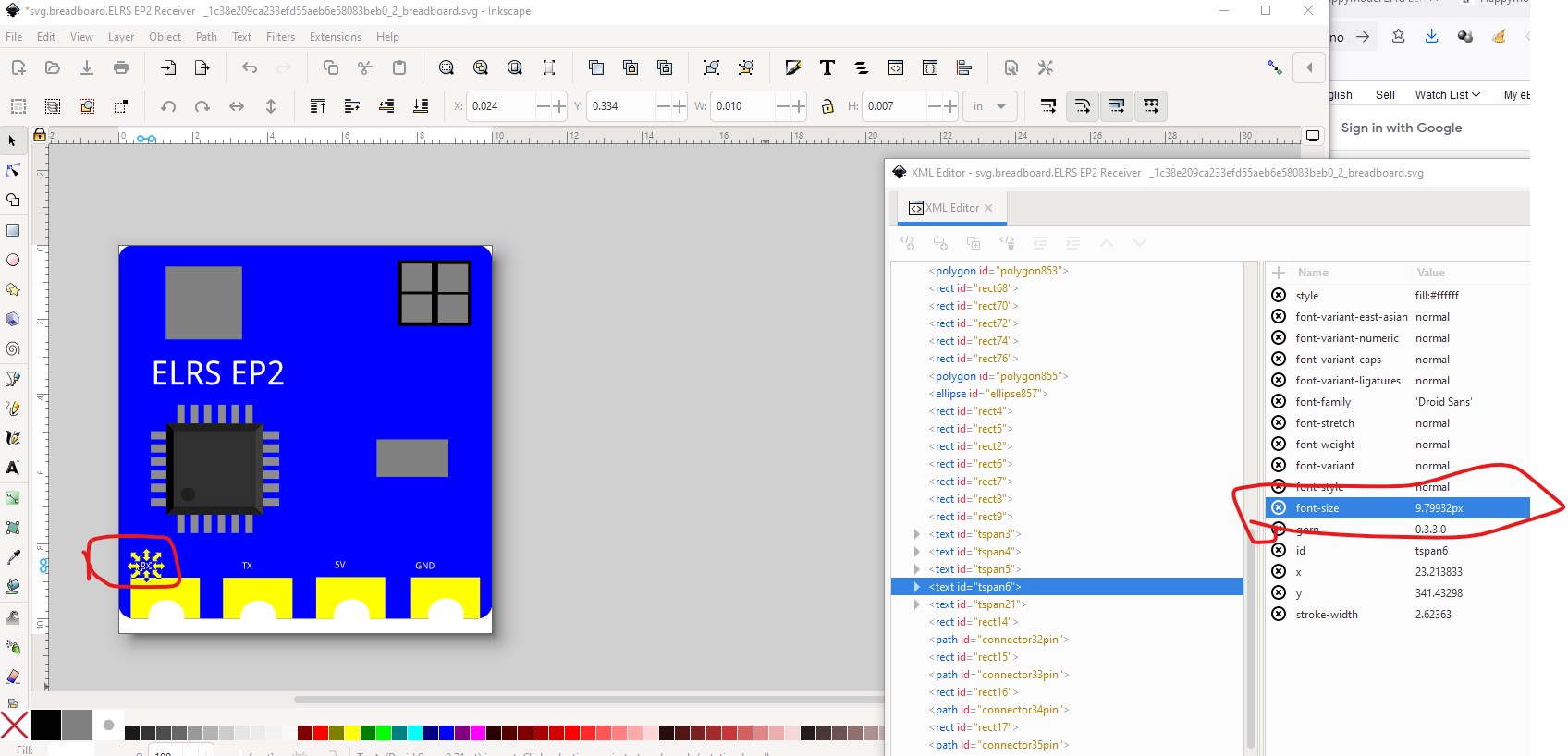
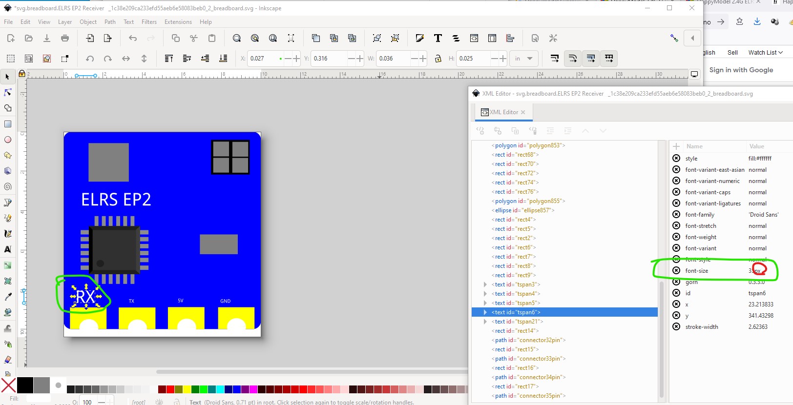
OK, first I think your font size problems are probably because you didn’t remove the px from the font size in the svg. If the font size has px on input to Fritzing it will sometimes (usually in part editor I think) set the font size to 0 or make it very large. You look to have gotten the small font problem (or set the wrong font size in your svg editor which is also a possibility). Pretty much everything I will do here is covered somewhere in this tutorial in the tutorials section of the forum.
specifically FritzingCheckPart.py (referenced there) will remove the px (among other things such as checking the part for errors) from the font size fixing the issue for Fritzing. For CSS compliance Inkscape (and possibly the other svg editors but I only know Inkscape) will add the px back in to the font size when editing a svg. That said lets look the breadboard svg in your part and point out issues.
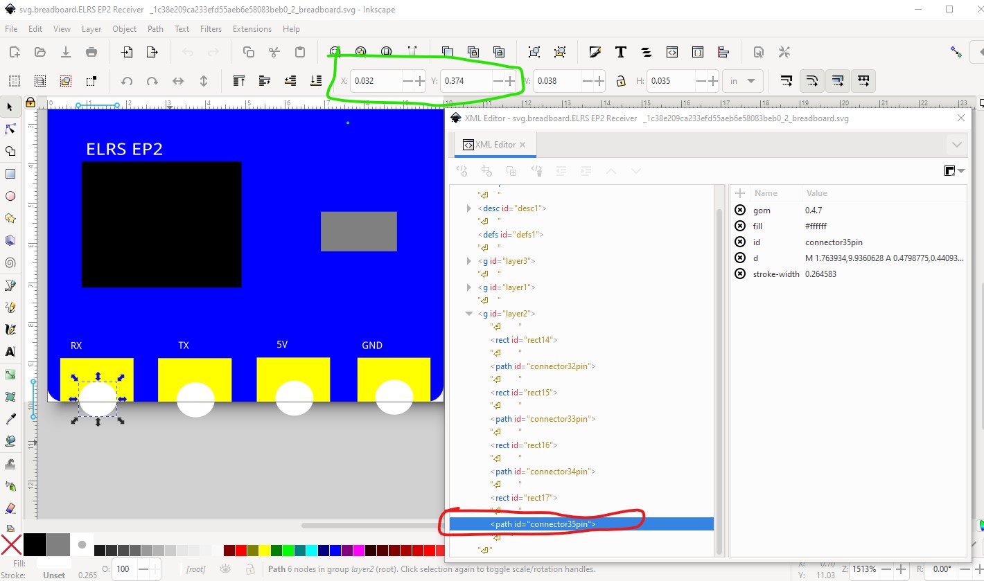
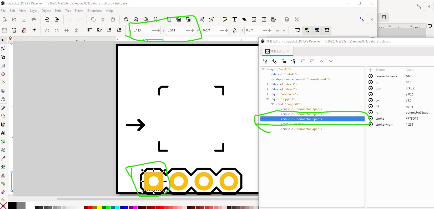
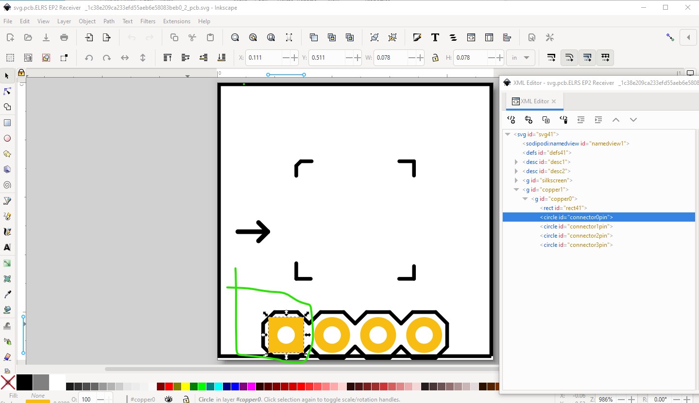
the pad should preferably be a circle rather than a path. A path will technically work but a circle makes things easier. The first problem is that these pads are not on 0.1in boundaries and presumably they should be to fit 0.1in headers. Using the x/y coords of the initial pad (circled in green on the top left of the image) we see that the next pad is not on a 0.1in boundary.
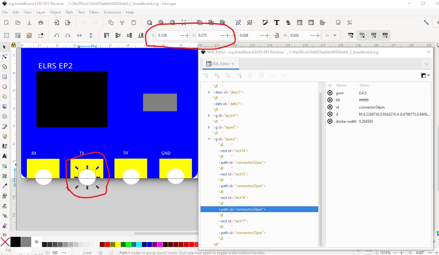
rather than x 0.132in y 0.374in the second pad is at x 0.129in (so a little short) y 0.375in (slightly down from what it should be.) that continues for the next two pads as well. Pcb is correctly spaced on 0.1in boundaries:
Here the font size (as always in Inkscape) has a px appended (circled in red on the left in xml editor) although it is the correct font size now that may not survive being loaded in to Fritzing as noted above.
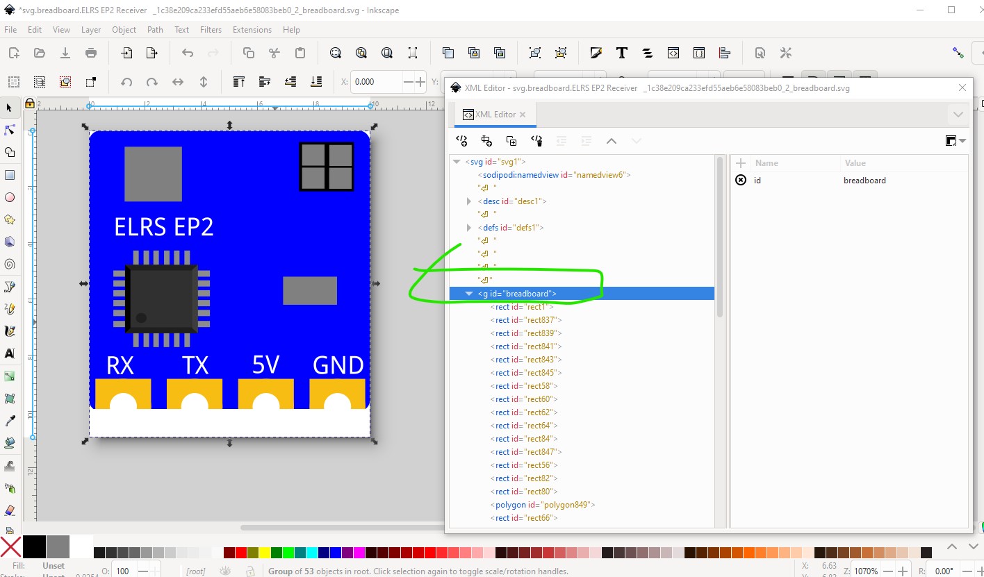
changing all of the font sizes to reasonable values and changing the pads to circles aligned on 0.1in boudaries and using a white rectangle to mask off the bottom half of the circles provides an accurate copy of the breadboard svg. As well I grouped the entire svg and set its id to breadboard to add the necessary layerId to the svg. Without the layerId the part will not export as an image.
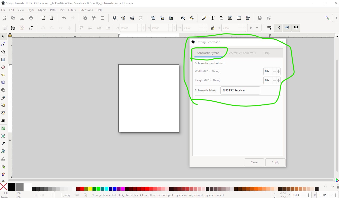
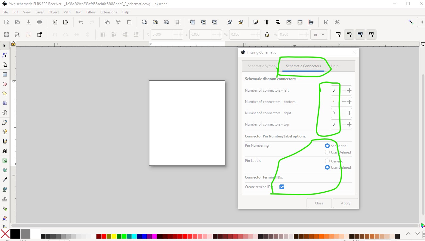
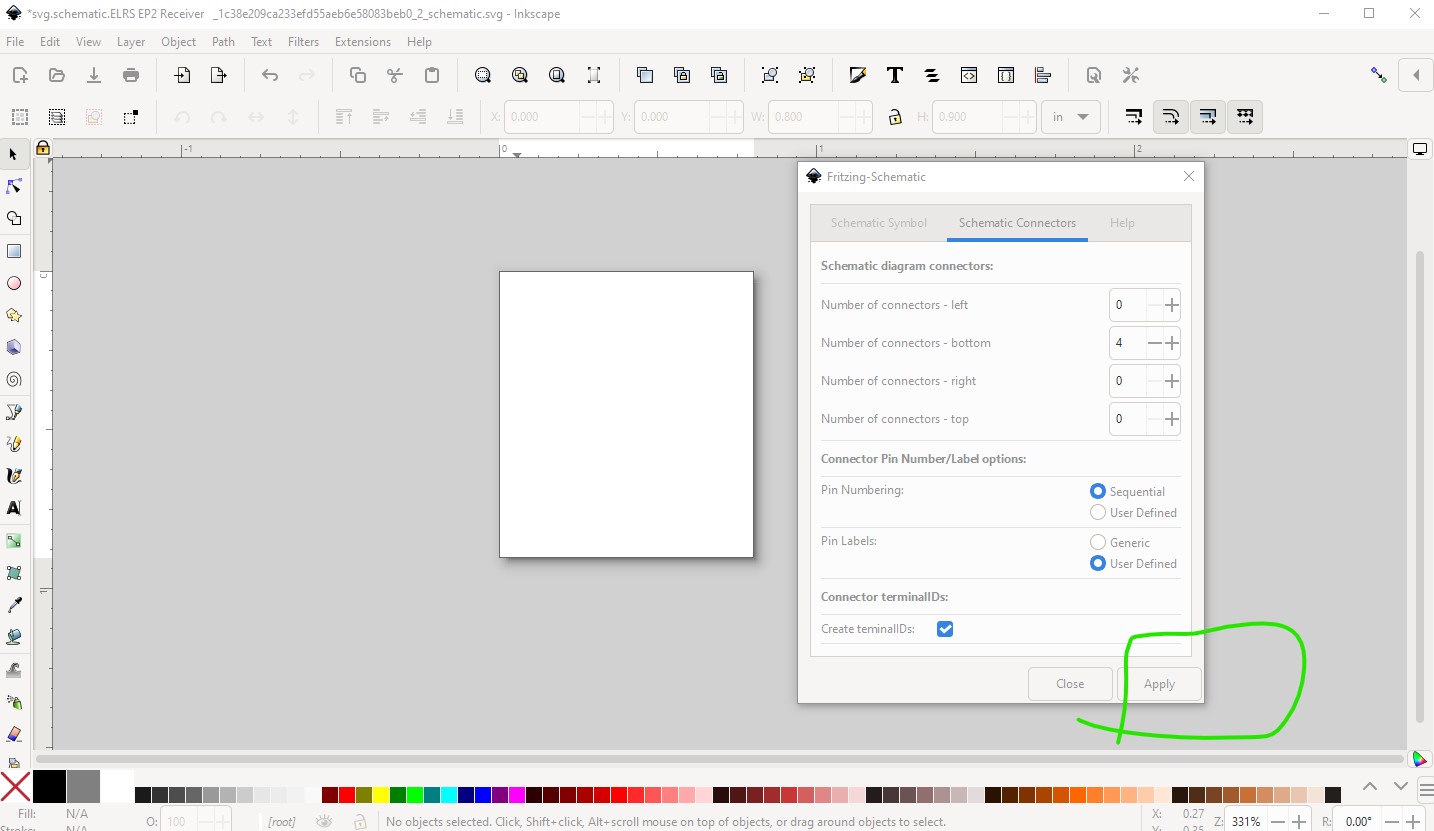
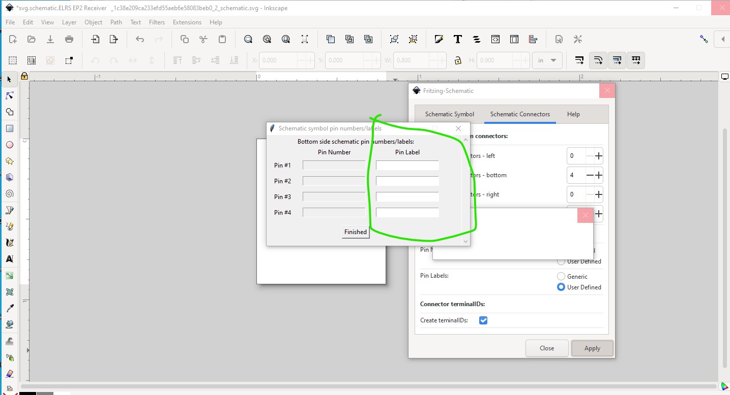
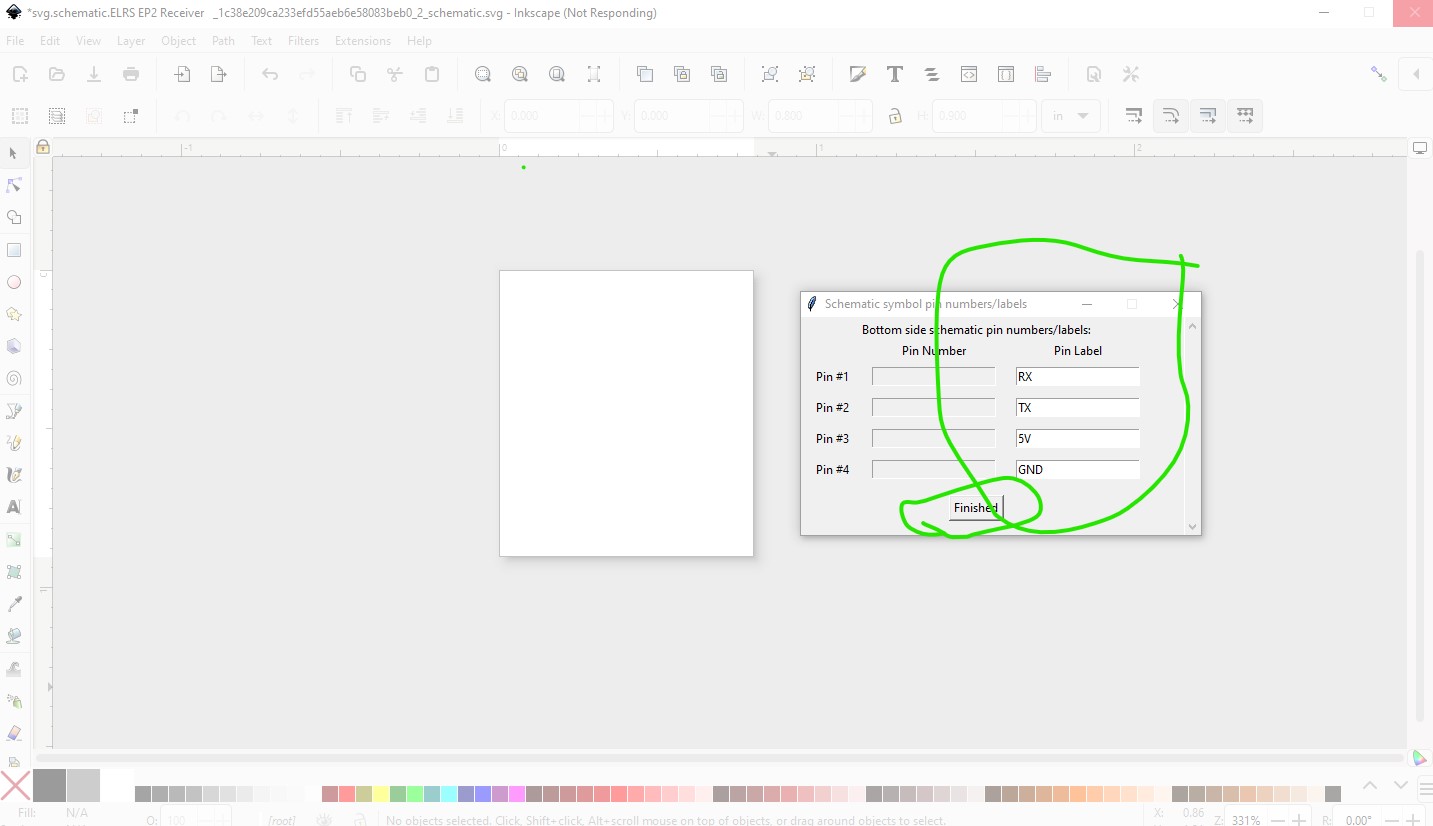
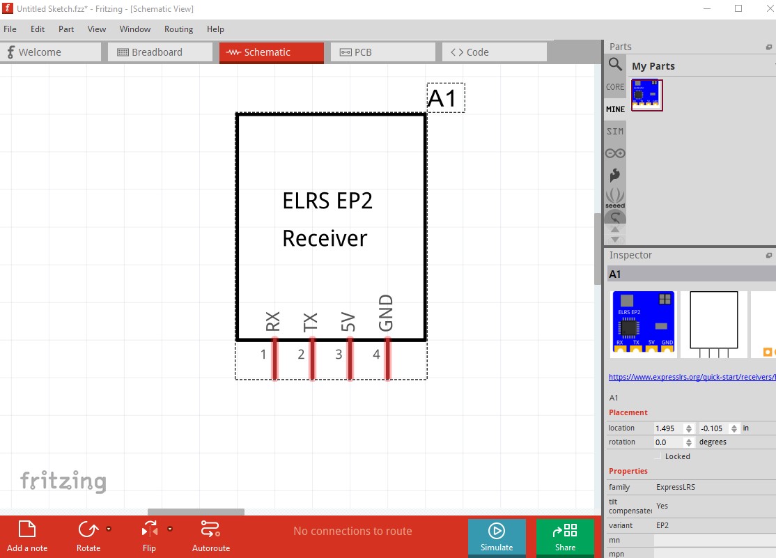
On to the schematic svg. Rather than use and modify your schematic I chose to use Randy’s Inkscape schematic generator extension to make a new schematic. This will automatically start the pins at 0 and produce a schematic that meets the graphics standards. Its use is covered in the tutorial above.
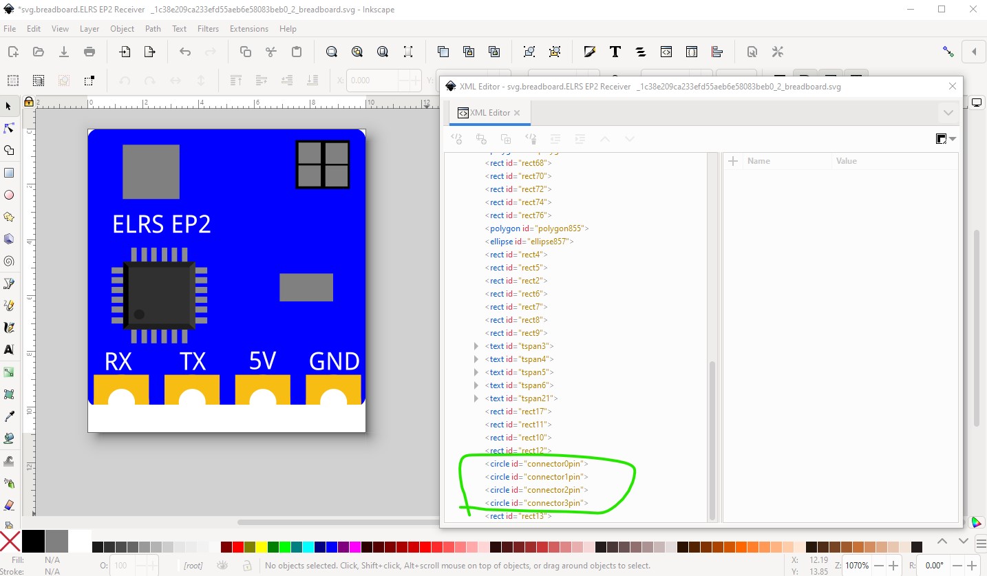
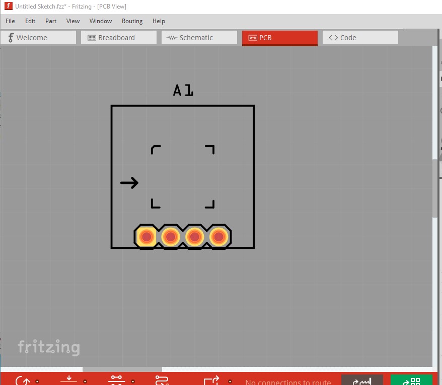
then save it as the new schematic svg. Now on to pcb. Here I cleaned up some and renamed the connectors to connector0pin to connector3pin (and later modified the .fzp file to match!)
save this as the pcb svg. Make the necessary modifications to the .fzp file and run the resulting part through FritzingCheckPart.py to remove the pxs from the font sizes and check for errors:
note if you have already downloaded this part you will need to delete the current part from Fritzing (then restart Fritzing answering yes to save parts and mine parts bin changes) before you will be able to load the new part.
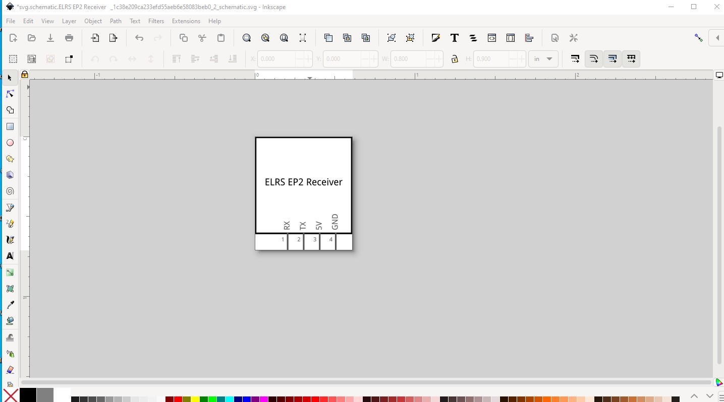
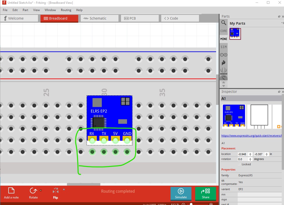
note I didn’t change the moduleId for this part so you will need to delete your current part then shutdown and restart Fritzing before it will let you load the new part. The new part looks like this in Fritzing:
I expect pcb won’t be that useful. It appears the usual use of this device is to solder wires to the pads on the board, but those wires will fit in to the holes (as will a 0.1in header if you want to be able to unplug it! Hope this helps and if anything is unclear feel free to post a question.
I noticed a problem with the dimensions of the pcb view. The pcb dimensions are 15mm x 15mm which does not match the breadboard view.
I changed the pcb svg dimensions in Inkscape which was intuitive. The problem is when I import the pcb svg back into FZ, I get an error that states, “This version of the new Parts Editor can not deal with separate copper0 and copper1 layers”. Then I am only able to connect to one terminal.
I did not change the copper terminal sizes. I only changed the copper location. Why do I get this error?
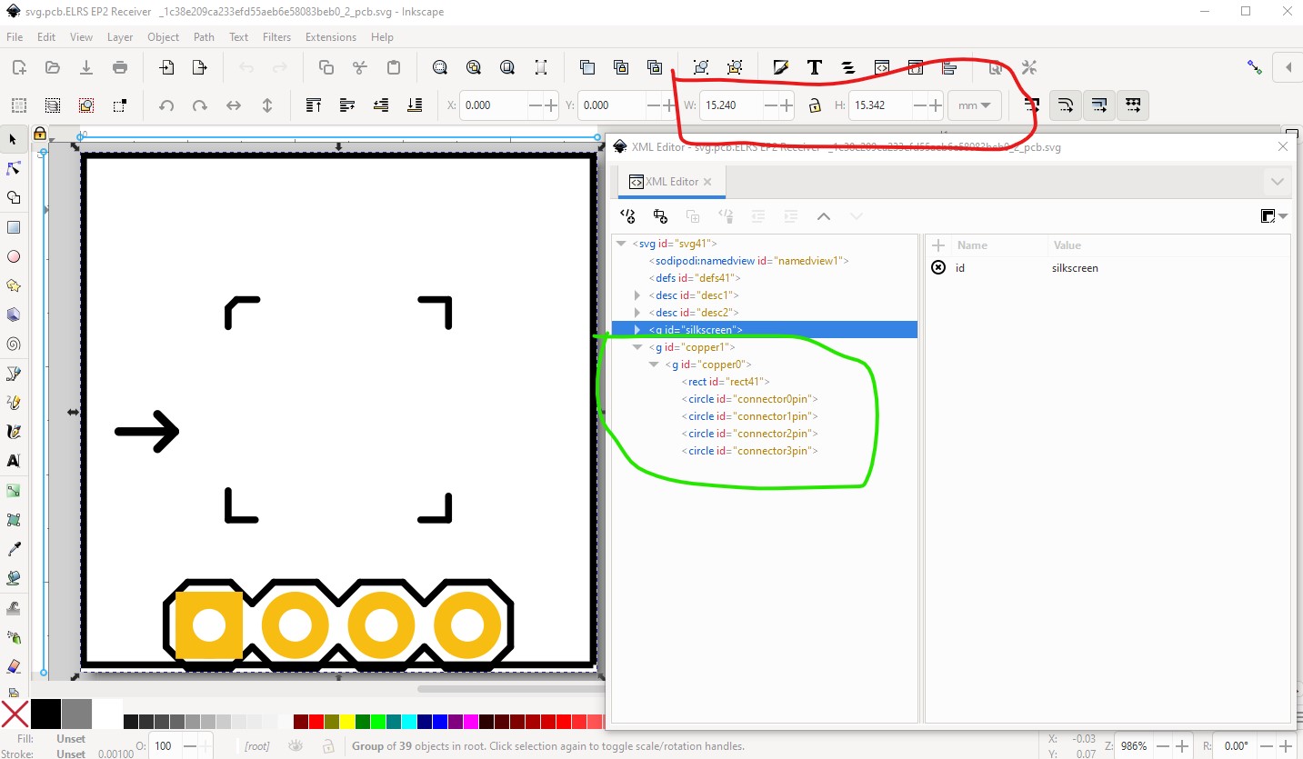
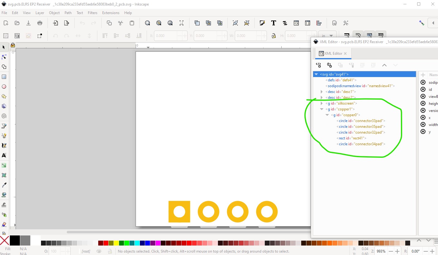
the error message you describe indicates that copper1 and copper0 are separate groups on the same level (which is an older format and may be in the original svg.) Your best bet would be to either upload your modified pcb svg (upload is 7th icon from the left in the reply menu, which accepts svg files) or the .fzpz for your modified part (but it sounds like you don’t have a .fzpz file as parts editor won’t load it.) I can also just correct the part to match breadboard which may be the easiest solution. The pcb svg in my fixed part looks like this:
the dimensions (circled in red here) are wrong they should be around 10mm by 10mm not 15mm by 15mm. The copper1/copper0 groups should look like this (circled in green)
It sounds like you probably started from the pcb svg file from the original part, nope that isn’t correct because the original is also correct so I don’t know how your pcb svg got corrupted.
I’ll have a look at modifying the pcb svg to match breadboard. The tutorial listed at the start of my post describes how I made the changes to the part (I typically don’t use parts editor to modify parts as it wasn’t finished when development stopped and hasn’t yet been updated.)
edit
As you will see I just updated the part with a corrected to match breadboard pcb svg in the original post. If you upload the svg you used to make the pcb svg I can tell you what is wrong with it (as enabling you to modify parts is very desirable!)