Difference between SVG/PDF and Gerbers

Hello all.

I created a part (smd) for fritzing and used it in a test circuit design just to make sure everything is OK. I get proper copper pads when I export the file in SVG and PDF.

pdf_export

When I try to export in Gerber format and inspect the file through an app (or even online at jlcpcb) I see that a couple of pads are too close.

gerber

Any ideas where I should be looking at?

I have attached the part in case anyone would like to have a go and compare the Gerber exports.

JDY-23 BLE 5.0 Module.fzpz (18.6 KB)

I recreated the part again. It seems the issue is now gone! I did had to correct some parts in the previous SVG file for the PCB view.

This is how it looks now in PDF export:
export_2

and how it looks in Gerber export:
export_1

Print testing looked fine.

I also uploaded the part in case somebody needs it.

JDY-23 Bluetooth LE Module.fzpz (14.2 KB)

Sorry for the late reply, I have been busy. Over all a good part but a few improvements. Most of the problem is a lack of termnalIds in schematic. Your current part looks like this:

note the wires connect to the middle of the pin (no terminalId defined) and the right and left pins are offset 0.05in from the grid (for the same reason!) Here is the schematic from my improved part which corrects these issues:

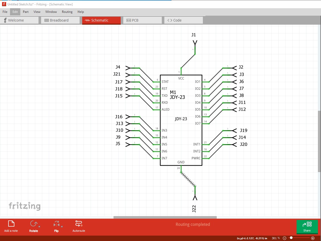
note schematic is slightly smaller than your original to get it to fit the grid correctly. As well breadboard and schematic svgs lack layerIds. That results in the part not exporting as an image (i.e a pdf, png, jpg etc.) Here is a list of all the things I changed in your original part:

bb

no layerId, wrong scale, pins don’t start at 0.

ungroup rescale

move connectors to the bottom of the svg renumber

schematic

no layerId wrong scale, origin not 0 0, pins mis aligned, incorrect colors and fontsize.

Replace with a schematic generated by Inkscape extension which will require a renumbering in breadboard.

I created the new schematic with this Inkscape extension:

pcb

silkscreen is not a group which it needs to be.

Renumber the pads to start at connector0 and end in pad to match schematic (needs changes to .fzp file)

fzp file

renumber the pins, remove the bus definition.

most of them make no visual or operational change, they just make the part conform to the parts standards. Here is the part with the above changes in it (I didn’t change the moduleId so you will need to delete your current part to be able to load this one!) Hope it helps. If anything isn’t clear feel free to ask.

JDY-23 Bluetooth LE Module-improved.fzpz (8.9 KB)

Peter

Hi Peter, than you for taking a look at my part.

I missed all those guides when I was creating the part to be honest, but I really like your details explanations which I will be using as a reference along with this part for any future parts I will be making.

Thanks again,
Stelios

I now have an updated version which also corrects the pad issue for this part. There is more space in-between the pads.

You can get it here:
JDY-23 Bluetooth LE Module.fzpz (12.8 KB)

Looks fine. FritzingCheckPart.py’s only complaint is that connector1 and connector2 are missing (they are the NC pads) to stay in sequence which isn’t a huge problem.

Peter

Hi Peter.

I didn’t get this error when going through each file before updating the part in the editor.
How can I fix that?

Also, I noticed that in my original PCB file I could see in the XML editor that I had strokes defined (style, color) but using a width of 0. This made the part look OK in Fritzing editor but in the gerber export and also after pcb manufacturing the stroke was messing the final pad sizes making them bigger. I removed every reference to stroke and the pads, at least in the gerber exports, look fine. Awaiting for the PCBs to arrive and check that too.

Stelios

Parts editor doesn’t enforce or check pin numbering (it in fact has some bugs which tend to skip pin numbers.) To fix it you would need to renumber the pins which is a fair amount of work as it needs to be done in the fzp file and all the svgs. It is probably easiest to leave them as is as it doesn’t usually hurt too much (sometimes hovering over a pin to display the pin description text will get the text for an incorrect pin is the only one I know of.)

If the 0 stroke with is on connectors you are going to get a board with no pads, just a hole. It is advisable to check the gerber output in a gerber viewer such as gerbv before ordering boards as gerber processing takes place after the pcb display in Fritzing and thus can be different than it appears in Fritzing. If you upload the .fzz file for your board I can look over the geber output and tell you if you are likey to have problems (upload is 7th icon from the left in the reply menu.)

Peter

Thanks for that Peter!
I got the PCB and was able to verify that the part is printed OK.
Should I re-post the part in the forum so it’s easy for other people to find it?

Probably better to edit the post above and replace the current part (if it has changed) so there is only a correct copy present.

Peter