How would one go about this? Is this the load image file button in the Inspector in PCB view when the PCB is selected?
Yes. That is how to get the outline attached to the board.
Right.
I’m not commissioned. It’s pure personal projects/prototypes. As it’s not finished and improving I review, design new boards, … I’m not commissioned at all to create a part or anything else by the providers. Because the Gerber files of the boxes are not public, I asked Camdenboss the authorization to work publicly on this putting diagrams, …
Well, the „commissioned“ was just an example to better illustrate the point of wanting to create something reusable for future similar boards. Instead of just a one-off project.
I think microMerlin summed it up pretty well how this could work, for the reuse scenario.
Thanks a lot to you all. Searching the forum differently I found this one which looks like what I want to achieve, except for holes but using a separate part can help to solve this.
How do you import a custom pcb shape in Fritzing, to make it available here :
thanks
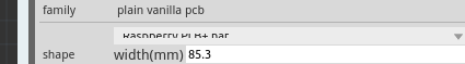
I can’t quite see what that drop-down says, but I think this is the one which will only list built-in, i.e. core board shapes. To use your own board shape use the load image file button just above that.