Constraint design of PCB board

Hi,

I have a PCB board with a specific design. Specific shape, cuts, and connector location.

(I designed it as an SVG file.)

I tried to use the image as board image but I can’t see the connector.
If I use it as a component, I don’t have the shape/cuts…

how would you do ?

Upload the fzz sketch with the 7th button in the reply.

Mayby this vid will tell you how to fix custom PCBs

That sounds like you are mixing up (together) the functions of a part (component) and pcb. An svg file used for a pcb image contains only cutout shapes and (maybe silkscreen). It will not have anything related to connectors or copper.

A part (component) has the copper pads, silkscreen, and (optionally) drill holes. The holes can be for through hole connections (when they have a copper border (svg stroke width), or mounting holes when not stroke exists. A common recommendation is to mark mounting hole location of a part using only silkscreen. That way the part can be used without the mounting hole when desired, and the silkscreen shows where to place a separate “hole” component when it is wanted.

You need a board svg, and a separate part (or multiple parts).

Ok, thanks. That’s a bit what I reached.
The only tricky thing is to align board and part.

Only tricky because the board does not do align to grid. Suggest putting a marker (silkscreen) on the board someplace that will be on the grid. Place a part (like a hole), align it to grid, then drag the board to match. Lock the board to keep it from moving, delete the part used to align the board, then place the real part.

To align connector on the grid, position the connectors on exact measures, like.

That works for aligning a connector (that is in a part) to the grid of the current view, or connectors within a part relative to each other. It does not work for aligning board image with the grid. If the image is not aligned to the grid, the connector of the part will not be aligned with the image either.

You can place the board image using exact coordinates, but you need to know what (if any) the offset is from the image reference point (corner) to the connector position that is to be lined up with the grid. That offset will be consistent for a single board image, but could easily be different for 2 different boards. once the board image is positioned correctly (and locked) then parts can be positioned using the standard snap (align to grid), without needing to be placed by exact coordinates.

Right, that’s a complex topic. Let’s do an example with a good mix of metrics and imperial systems.

  • Card dimensions: 70mm x 60mm
  • 2 Mounting holes of 4mm at 10mm of the borders in each corners.
  • 10 connectors, 1mil spaced on each longest side at 2inches of each other, hole diameter 1mil copper size 0.5mil, first hole at 23mm of a border

Can you complete the svg file, add others to create a component … ?
thanks

For 72dpi, the SVG would be but it’s not aligned in Fritzing:

<?xml version='1.0' encoding='UTF-8' standalone='no'?>
<svg baseProfile='tiny'
	 height="60mm"
	 version='1.2'
	 viewBox='0 0 1984.25 1700.78'
	 width='70mm'
	 x="0"
	 xmlns='http://www.w3.org/2000/svg'
	 y="0">
			<g id="silkscreen">
				<rect x="0" y="0" width="1984.25" height="1700.78" fill="none" stroke="#000000" stroke-width="1"/>
				<circle cx="283.46" cy="283.46" fill="black" id="nonconn0" r="56.69" stroke="#f9a435" stroke-width="0"/>
				<circle cx="1700.79" cy="283.46" fill="black" id="nonconn0" r="56.69" stroke="#f9a435" stroke-width="0"/>
				<circle cx="283.46" cy="1417.32" fill="black" id="nonconn0" r="56.69" stroke="#f9a435" stroke-width="0"/>
				<circle cx="1700.79" cy="1417.32" fill="black" id="nonconn0" r="56.69" stroke="#f9a435" stroke-width="0"/>
			</g>
	<g id="copper0">
		<circle cx="651.96" cy="130.39" fill="none" id="pin1.1" r="15.59" stroke="#f9a435" stroke-width="7.08"/>
		<circle cx="723.96" cy="130.39" fill="none" id="pin1.1" r="15.59" stroke="#f9a435" stroke-width="7.08"/>
		<circle cx="795.96" cy="130.39" fill="none" id="pin1.1" r="15.59" stroke="#f9a435" stroke-width="7.08"/>
		<circle cx="867.96" cy="130.39" fill="none" id="pin1.1" r="15.59" stroke="#f9a435" stroke-width="7.08"/>
		<circle cx="939.96" cy="130.39" fill="none" id="pin1.1" r="15.59" stroke="#f9a435" stroke-width="7.08"/>
		<circle cx="1011.96" cy="130.39" fill="none" id="pin1.1" r="15.59" stroke="#f9a435" stroke-width="7.08"/>
		<circle cx="1083.96" cy="130.39" fill="none" id="pin1.1" r="15.59" stroke="#f9a435" stroke-width="7.08"/>
		<circle cx="1155.96" cy="130.39" fill="none" id="pin1.1" r="15.59" stroke="#f9a435" stroke-width="7.08"/>
		<circle cx="1227.96" cy="130.39" fill="none" id="pin1.1" r="15.59" stroke="#f9a435" stroke-width="7.08"/>
		<circle cx="1299.96" cy="130.39" fill="none" id="pin1.1" r="15.59" stroke="#f9a435" stroke-width="7.08"/>
		<circle cx="651.96" cy="1570.39" fill="none" id="pin1.1" r="15.59" stroke="#f9a435" stroke-width="7.08"/>
		<circle cx="723.96" cy="1570.39" fill="none" id="pin1.1" r="15.59" stroke="#f9a435" stroke-width="7.08"/>
		<circle cx="795.96" cy="1570.39" fill="none" id="pin1.1" r="15.59" stroke="#f9a435" stroke-width="7.08"/>
		<circle cx="867.96" cy="1570.39" fill="none" id="pin1.1" r="15.59" stroke="#f9a435" stroke-width="7.08"/>
		<circle cx="939.96" cy="1570.39" fill="none" id="pin1.1" r="15.59" stroke="#f9a435" stroke-width="7.08"/>
		<circle cx="1011.96" cy="1570.39" fill="none" id="pin1.1" r="15.59" stroke="#f9a435" stroke-width="7.08"/>
		<circle cx="1083.96" cy="1570.39" fill="none" id="pin1.1" r="15.59" stroke="#f9a435" stroke-width="7.08"/>
		<circle cx="1155.96" cy="1570.39" fill="none" id="pin1.1" r="15.59" stroke="#f9a435" stroke-width="7.08"/>
		<circle cx="1227.96" cy="1570.39" fill="none" id="pin1.1" r="15.59" stroke="#f9a435" stroke-width="7.08"/>
		<circle cx="1299.96" cy="1570.39" fill="none" id="pin1.1" r="15.59" stroke="#f9a435" stroke-width="7.08"/>
		<g id="copper1">
			<circle cx="651.96" cy="130.39" fill="none" id="pin1.1" r="15.59" stroke="#f9a435" stroke-width="7.08"/>
			<circle cx="723.96" cy="130.39" fill="none" id="pin1.1" r="15.59" stroke="#f9a435" stroke-width="7.08"/>
			<circle cx="795.96" cy="130.39" fill="none" id="pin1.1" r="15.59" stroke="#f9a435" stroke-width="7.08"/>
			<circle cx="867.96" cy="130.39" fill="none" id="pin1.1" r="15.59" stroke="#f9a435" stroke-width="7.08"/>
			<circle cx="939.96" cy="130.39" fill="none" id="pin1.1" r="15.59" stroke="#f9a435" stroke-width="7.08"/>
			<circle cx="1011.96" cy="130.39" fill="none" id="pin1.1" r="15.59" stroke="#f9a435" stroke-width="7.08"/>
			<circle cx="1083.96" cy="130.39" fill="none" id="pin1.1" r="15.59" stroke="#f9a435" stroke-width="7.08"/>
			<circle cx="1155.96" cy="130.39" fill="none" id="pin1.1" r="15.59" stroke="#f9a435" stroke-width="7.08"/>
			<circle cx="1227.96" cy="130.39" fill="none" id="pin1.1" r="15.59" stroke="#f9a435" stroke-width="7.08"/>
			<circle cx="1299.96" cy="130.39" fill="none" id="pin1.1" r="15.59" stroke="#f9a435" stroke-width="7.08"/>
			<circle cx="651.96" cy="1570.39" fill="none" id="pin1.1" r="15.59" stroke="#f9a435" stroke-width="7.08"/>
			<circle cx="723.96" cy="1570.39" fill="none" id="pin1.1" r="15.59" stroke="#f9a435" stroke-width="7.08"/>
			<circle cx="795.96" cy="1570.39" fill="none" id="pin1.1" r="15.59" stroke="#f9a435" stroke-width="7.08"/>
			<circle cx="867.96" cy="1570.39" fill="none" id="pin1.1" r="15.59" stroke="#f9a435" stroke-width="7.08"/>
			<circle cx="939.96" cy="1570.39" fill="none" id="pin1.1" r="15.59" stroke="#f9a435" stroke-width="7.08"/>
			<circle cx="1011.96" cy="1570.39" fill="none" id="pin1.1" r="15.59" stroke="#f9a435" stroke-width="7.08"/>
			<circle cx="1083.96" cy="1570.39" fill="none" id="pin1.1" r="15.59" stroke="#f9a435" stroke-width="7.08"/>
			<circle cx="1155.96" cy="1570.39" fill="none" id="pin1.1" r="15.59" stroke="#f9a435" stroke-width="7.08"/>
			<circle cx="1227.96" cy="1570.39" fill="none" id="pin1.1" r="15.59" stroke="#f9a435" stroke-width="7.08"/>
			<circle cx="1299.96" cy="1570.39" fill="none" id="pin1.1" r="15.59" stroke="#f9a435" stroke-width="7.08"/>
		</g>
	</g>
</svg>

The viewBox value looks ‘odd’ for something using drawing dimensions of 60 by 70 mm. A little math says that was probably created using 720 px per inch, then converted to mm. Or actually, the 60 by 70 mm was converted to inches, then the drawing done at 720 px per inch, and results switched back to mm.

That works. I normally do new graphics using either 1000 px per inch (1 px = 1mil), when working in inches, or 100 px per mm when working in mm. That makes most of the coordinate numbers simpler for the general cases.

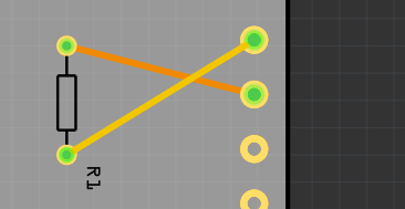
Since it contains silkscreen, copper0, copper1, that appears intended to be the graphic to use in a part definition. A bit unusual, in that the top and bottom connector circles are duplicated, AND the copper1 is inside copper0. Extracted and truncated, that should be something like either:

<g id="copper0">
  <circle cx="651.96" cy="130.39" fill="none" id="pin1.1" r="15.59" stroke="#f9a435" stroke-width="7.08"/>
  <circle cx="723.96" cy="130.39" fill="none" id="pin1.1" r="15.59" stroke="#f9a435" stroke-width="7.08"/>
</g>
<g id="copper1">
  <circle cx="651.96" cy="130.39" fill="none" id="pin1.1" r="15.59" stroke="#f9a435" stroke-width="7.08"/>
  <circle cx="723.96" cy="130.39" fill="none" id="pin1.1" r="15.59" stroke="#f9a435" stroke-width="7.08"/>
</g>

for distinct elements (not good for tht), or

<g id="copper1">
  <g id="copper0">
    <circle cx="651.96" cy="130.39" fill="none" id="pin1.1" r="15.59" stroke="#f9a435" stroke-width="7.08"/>
    <circle cx="723.96" cy="130.39" fill="none" id="pin1.1" r="15.59" stroke="#f9a435" stroke-width="7.08"/>
  </g>
</g>

for a single element that exists on both sides (standard tht)

For this to be used in a part, the circles in the copper groups would need connector«number»pin ids matching the part definition. To get some graphics to work with, this is fine, though technically, the id values should be unique.

All of the graphics for silkscreen should be black. fill and/or stroke as needed for the element. The stroke for the boundary rectangle is not large enough to be seen. The start and dimensions also need adjusting to be fully within the part. Half of the stroke is drawn inside, half outside of the specified edges, so starting from 0, 0 means half the stroke is missing.

Was your intent to have holes drilled (by the board producer) for the silkscreen circles? Given the earlier conversation, I thought that the intent was to not define holes for the part, but define them for the board instead. Also, the general (not fixed) recommendation for most parts, is to create them without mounting holes. That way they can be used in cases where the mounting holes (or only some of them) are not wanted in a project. The holes can always be added to the project, by using the ‘hole’ part. Just need to mark the silkscreen (typically a “+”) so that the hole can be added accurately. If they are in the part, they can not be removed from the project.

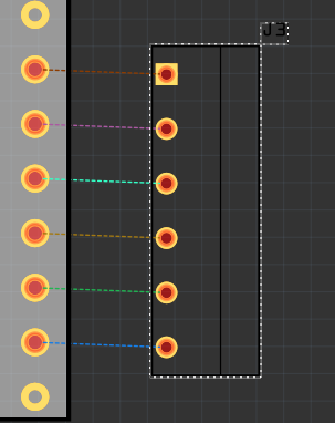
I see nothing here to base the board image on, which is what the part would need to align to. Or, since (most) parts are easy to align to the grid, it is the board image which needs aligning. What we need for a sample case is 2 images. One for the board, the other for the part. With a know common point that they need to align too.

I think we’ll have to make a documentation and maybe some tools to make and check file format and rules… :wink:

Yes, that’s what I want(ed). Your point is very interesting, but if I want the board with no holes, it has other dimensions. So I guess I would have to create another part.

I knew I should tried to import this file (thanks)

Right, I converted mm to inch dividing per 2.54. It seems time has no effect on my old mistakes…

I discovered that when the connector order changed in the designer. thanks.

I don’t really understand what you mean. in the silkscreen, should we have all elements filled, with or without a stroke ?
<circle cx="723.96" cy="130.39" fill="black" id="pin1.1" r="15.59" stroke="#000000" stroke-width="7.08"/>
or
<circle cx="723.96" cy="130.39" fill="black" id="pin1.1" r="15.59"/>

That’s a bit the goal of the example. I’m actually considering 2 options:

  • either use top left alignment for the board and the part.
  • or add an extra connector aligned on the grid as first connector

Let’s make things clearer (since Camdenboss is agreeing). I’m doing a Camdenboss board for their CNMB serie.

Here it the specification

The actual state of my part:
cnmb_c4a9aa2d32a2c11cfd95d0d1f5569774_20_pcb cnmb_c4a9aa2d32a2c11cfd95d0d1f5569774_20.fzp (17.5 KB) cnmb_c4a9aa2d32a2c11cfd95d0d1f5569774_20_schematic

What is done (and checked):

  • card dimension
  • screw hole positioning
  • connector positioning
  • connection works both sides: image

What remains:

  • being able to choose the size of the holes
  • choose between the two mounting variants (so far I only made the screw one)
  • maybe review the dpi by a factor 10
  • check part’s rules (color, file structure, …)
  • print exclusion area on the board

Actual problems:

  • when I import the pcb svg the link is not made between ui connectors and connectors. Even if I changed them, save, … it doesn’t keep the change. right and left connectors are associated to the same circles
  • exclusion area around hole does not display properly. Should be this: image
  • If I use a connector and tries to put it in the hole on the board, it doesn’t connect: image

Question:

  • will the connector be drilled by the board maker ?
  • will the mounting hole be drilled by the board maker ?
  • Is it supported to add parts over the board part ? will this works for a card provider to make the card ?

With fill or stroke or both are all valid. The point was that the color of whatever is used should be black, either the named color or the numeric equivalent is fine. Brought up because the initial example had stroke="#f9a435". The stroke-width was 0, so it did not actually have any effect. For that, I would change the stroke to “none”, and remove the stroke-width completely.

There seems to be 2 separate conversations happening here about different things. This post started with talking about a custom pcb image, and getting parts to line up correctly with it. Now it seems to be about creating a part, without any reference to a custom pcb image.

For your part, not enough has been included to see how things are interacting. The fzp is the definition, but it is used in combination with the referenced svg view files to get the functionality. Without those, we can not see what might be causing the symptoms you describe. The easiest way to include them, is to post (upload) the fzpz file. It include the fzp and svg combined into a single file. The file is really a zip, so it is easy to extract the individual files again. If you are using the Parts editor, and can not get it to create the part, the set of fzp and svg files can be put in a zip, then renamed to .fzpz, which can be uploaded here.

Checking parts rules: There is a FritzingCheckPart tool available to do some automated checks. At least initially, work with a copy of your part files in a separate folder. The current version makes changes to files, and you might not want that, until you see what it does. You can work from the reported problems on your originals instead. Not everything it reports is necessarily an error. But most should be investigated.

Exclusions are is (AFAIK) done with silkscreen content. I have seen a “keepout” layer in fritzing part file documentation, but do not know just how it works.

Connectors will be drilled (if the rest of the part is correct) when the connector«number»pin element is a circle. The size of circle, combined with the stroke width determine the size of the hole. To verify what the board house will ‘see’, you need to place the part on a project, export it in gerber format, then use a gerber viewer on the resulting set of files.

If it is a circle, the mounting hole will be included in the drill list. It will be plated through only if the hole has a stroke width.

Your last about parts, board, card need to be elaborated some to be clear. If I understand, it all comes down to the 3D clearances on the different parts. Which Fritzing has no knowledge of. The pcb in Fritzing can be created using multiple parts, that can be positioned anywhere. Overlaping or not. The board will be created however it is laid out. It will only actually work if the parts used actually fit, and do not interfere with each other. It is up to the creator (Fritzing user) to make sure that what is being designed makes sense. The board maker (production house) will just create whatever is sent to them, normally as gerber files.

To demonstrate symptoms in Fritzing, you can upload the fzz file here. That includes the parts used in the Sketch, so it is also an alternative to uploading the fzpz file. Screen shots often only tell some of what is happening.

Many thanks @microMerlin for your help

This part is the famous board with constrained location of the screw and connectors…

So far I haven’t shared the fzpz, because it don’t load in Fritzing. as soon as I have it working, I upload it.

While it is correct that FritzingCheckPart.py currently modifies the file, it leaves the original file in filename.bak (because the error message line numbers refer to the input file, not the pretty printed modified output file.) Running FritzingCheckPart.py twice (without renaming the .bak file) will destroy the original so saving a copy of the original is the safest bet.

For hole sizes the drill.txt file will give the in size of all holes (although finding out what hole it refers to can be a challenge!) If you are using Inkscape as your svg editor the hole size is set by hole size = pad-diameter - (2 * stroke-width) So for an svg at the recommended scale for a .1in header which wants an 0.038in hole, with a 20 thou ring thickness, the pad diameter wants to be 0.078in.

0.078 - (2 * 0.02) = 0.038 and the gerber drill.txt file will have a 0.038in hole specified.

Feel free to upload the non working .fzpz file and one of us will correct it so Fritzing is happy with it and repost it for you. There are a lot of constraints which check part tries to deal with but sometimes it misses (and since I wrote it, I can usually figure out what is wrong.) There are some Camdenboss parts in core parts so exporting one of those as an fzpz file (right click on the part and select export part) then unzipping the fzpz file will give you the files of a working part to use as an example.

Peter

I still have the suspicion that everyone is not talking about the same thing. Looking at your part rather fuels that suspicion.

Maybe it would be good if you could explain what your actual goal is, what it is that you want to achieve. In real, outside of Fritzing. Maybe Fritzing isn’t the right tool for the job.

I want to use Camdenboss CNMB box for a project.

These boxes have a specific pcb dimensions, screw and connectors locations. The shape here is a simple rectangle with dimensions are in mm.

I also have to position some components on the pcb board at specific position regardless of the inch grid. Draw on the pcb or only display in Fritzing some exclusion/“keep out” areas.

For those reasons, I would like to have a “predefined” board with all that, to avoid having to reposition every time these elements on the board.

That description is not enough to figure out what you are using, or what the project needs (in Fritzing). Do you have a link to the (datasheet for the) actual box? Is that a pre-wired board? Is the project going to (also) need a separate pcb board that will be manufactured separately based on the holes and traces to be placed and drawn in Frtizing? Something created from gerber files exported from Fritzing.

If no separate pcb is needed, and you are just adding parts (headers, terminals, components to the Camdenbos board (probably) no predefined board is needed for Fritzing.

If you are creating a custom pcb from the Fritzing Gerber files, that needs to match the format of the Camdenbos board (I assume the image discussed early in this thread), then you need that (svg) image to “load into” the standard Fritzing pcb part. That is not a custom part. It is just an image of the shape of the board, including cutout areas (mounting holes etc.), but NOT connectors that will be need by parts that will be mounted on the board. The image can also include silkscreen content, which can be used to (among other things) mark (but not enforce) keepout areas. If there are standard headers (screw terminals and more) that go with that, then they can be created as (one or more) custom Fritzing parts (with the connectors), but they can not be INCLUDED in the pcb image file. Fritzing parts can overlap each other without problems (in Frtizing). Fritzing does not track anything related to the size and boundaries of parts, other than the connectors to it. So a single part could be created with all of the standard (connectors for) terminals. Then only that part would need the extra work to position exactly where it needs to be to match the predefined board constraints. That part is still separate from the the image of the board.

You will also need a “process” to get the pcb positioned so that the added parts end up at the right place. More details are also needed for what you mean by:

Are the component locations (actually the connector pins) not on some sort of grid? The size and units of the Frtitzing view grid can be adjusted. For “keep out” areas, is that for component interference, or for traces (and other copper areas) on the pcb?

This will be a lot faster, and much more likely to be correct, if you take some time to collect and provide more details.

From what I gather, you have a certain housing, and you want to generate a PCB for a project that will be mounted into that housing. For this, the PCB needs drill holes at a fixed position, and also plated through holes at other fixed positions, because the housing comes with connectors that get mounted on a PCB destined for the housing. Is that correct?

What is not clear, is if this is a one off personal project and you only need to create this one PCB, on which more components are to be placed. Or, if this is work to create something like a template to create generic PCBs for different projects. Like, for example, maybe you got commissioned by someone to “add CNMB boxes” to Fritzing. Because the two scenarios could be solved differently.

Independently, one comment on the part that you uploaded. You have numbered the connector ids with non-consecutive numbers. (connector1pin, connector2pin, … connector8pin, connector11pin,…) This is usually not a good idea. The connectorXpin labels inside the part are internal and should be consecutive numbers for the X. These are independent from any names that you give the connectors, which are the ones shown to the user by Fritzing.

Expanding on that, “connector” is used in the Fritzing context. That is an electrical connection that is associated with copper traces and pads on a pcb board. Mechanical connectors, and other mounting hardware and holes are separate.

A variation that might get closer to what you want, is to have a board outline svg to load into the Fritzing pcb part. This image would not have any of the interior circular mounting holes, or anything related to where copper will or will not be. The edges of that image WILL provided a keepout limit, where the Fritzing “Design Rules Check” will complain if part (pin) connectors or traces get too close.

In addition to that, create a custom part that has the fixed header pin connectors, plus all of the holes for the main board. The image plus that part would combine to create what I think you want. The process for getting the initial pcb view setup would (could) be: load the pcb image, place and position the part (using whatever appropriate grid alignment, lock the part position, position the custom pcb based an coordinates of (offset from) the custom part, lock the pcb position. That should result in a pcb view that other parts and traces can be safely added to, with DRC complaining about any copper that gets too close to board edges, or the holes included in the custom parts.

If you want to avoid the repeated fiddly work of getting the part lined up with the pcb image, create a sketch that contains only that pcb image and part. Save that, and use it as a template for any project that uses that board / box.