Does anyone have the .fzpz of this 2A 5V charge discharge module?
Hi, this is my best attempt
2A 5V 4in1 Li-ion Battery Charger Discharge Module 3.7V 4.2V Charge Boost Board_WIPpcbgotproblem.fzpz (19.0 KB)
I have difficulties creating pcb becuz I dunno how long and wide the part is but breadboard and schematic working fine but schematic a bit misaligned… May need help…
Could you pls state the dimensions of the part? Thanks!
Here is a corrected part and how I got there.
2A 5V 4in1 Li-ion Battery Charger Discharge Module 3.7V 4.2V Charge Boost Board-fixed.fzpz (7.8 KB)
(note I didn’t change the moduleId of this part so you will need to delete the current part from your mine parts bin, then shut Fritizing down answering yes to the save parts and save parts bin prompts during shutdown to actually delete the part, then restart Fritzing before it will let you load the new part.
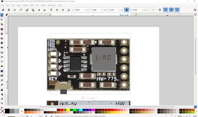
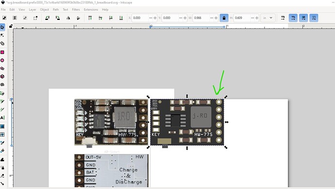
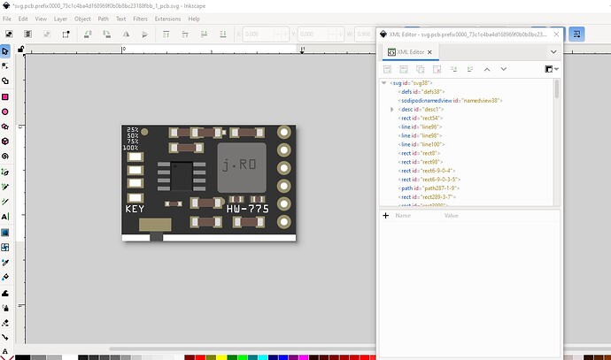
I started from your original breadboard svg which looked mostly fine (a few unneeded parts mixed in that I removed.) I grabbed the jpeg image from the ebay web site and imported it in to Inkscape then scaled it until it matched the connectors (which are on 0.1in centers and thus we know their size.) I deleted the path and rectangle and replaced it with a single rectangle (to make pcb easier later.) Then adjust the size and placement of the parts in breadboard to match the jpeg image that is overlaid on the breadboard svg (with the rectangle at the rear so the image shows above the base to place the parts.)
this is the jpeg image on the left and the new breadboard on the right
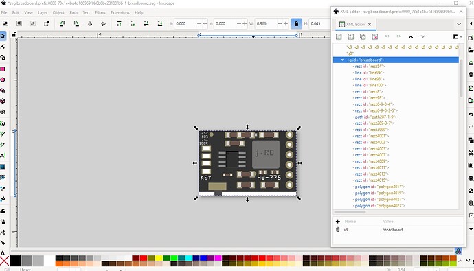
Your original part was missing the breadboard layerId (which causes the part to not export as an image.) so I added that like this, basically by doing Edit->select all then Object group to form the group and named it breadboard (to match the .fzp file definition.)
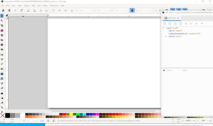
With breadboard finished I changed to pcb, and deleted everything. Then did a copy/paste in Inkscape of breadboard to pcb (a file copy will do the same thing if you copy the breadboard svg to the pcb svg.)
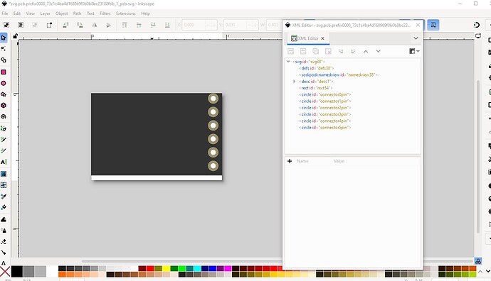
after copying the breadboard image, ungroup it to leave only the elements
then delete all the components except the base and the connectors.
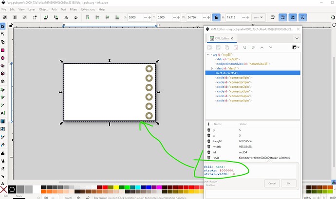
Now select the base rectangle, set its fill to none, stroke #000000, and stroke-width 10.
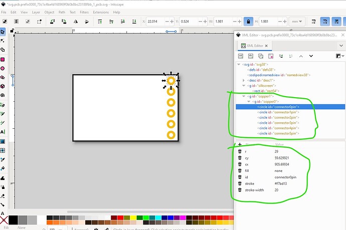
that sets the silkscreen. Then modify all the connectors to set the fill from #ffffff to none and the stroke to #f7bd13 which are the correct values for connectors in pcb. The radius and stroke-width (29 and 20) are correct from breadboard for 0.1in headers.
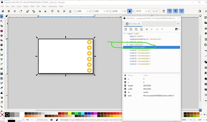
then select all the connectors and group them twice and name the goups copper1 and copper0 like this.
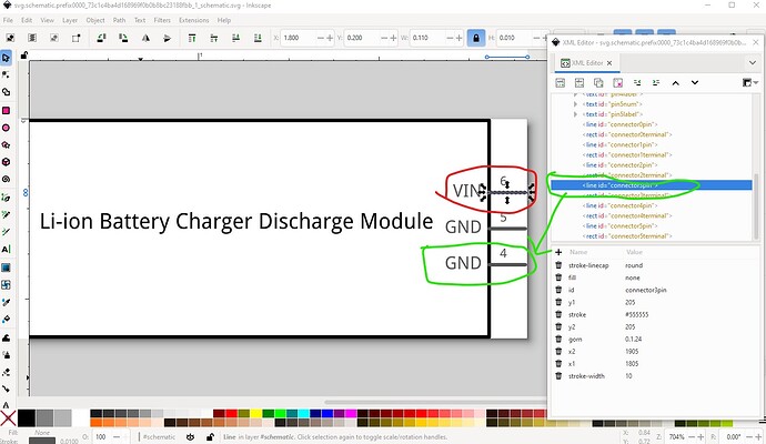
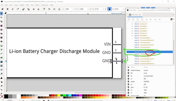
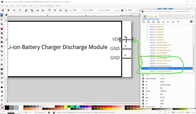
At this point (actually when testing the finished part) I discovered there is an error in schematic. The pins are defined in the wrong order. Connector3 is defined as what should be connector5 connector4 is correct and connector3 should be connector5 so make those changes.
here the pin is in the correct location but has the wrong labels.
so correct the labels so the pins are in the correct order./
then save the svg and rebuild the part and test it. That is the corrected part above and how it got that way. Hope this helps. All this information is in this tutorial if you haven’t seen it (it gets posted here lots ![]() )
)
Peter
Wow, thank you all so much for the dedication!
