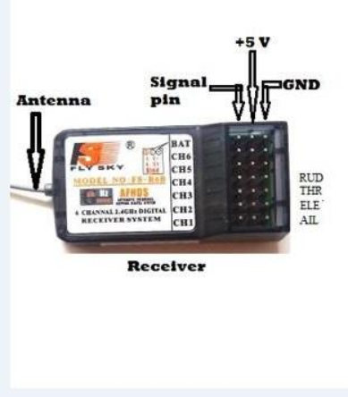
I need a part of a RC receiver …Model no flysky R6B
anyone please help
Your timing was good. I just finished a part for someone else with a bunch of servo connections making this relatively easy.
edit: Changed to add pcb as pads suitable for header connectors. Female allows it to plug in to the receiver, male or none to connect via wires.
flyskyr6b.fzpz (9.1 KB)
Peter
1 Like
ha ha ha thanks peter . but thing is it doesn’t work in pcb. I need pins in pcb.
I didn’t figure it would fit on a pcb very easily, but it is easy enough to add. I expect you don’t need much more than the 6 signal wires and a VCC and ground connection (as opposed to the complete set of 3 terminal servo connections each with VCC and ground?) as presumably that would more easily fit in to the connectors on the receiver. The difference looks like this:
The top example is a copy of the receiver servo connections without the battery connections (I’m assuming you don’t need them on the board, perhaps incorrectly) which takes the most space and is hardest to route on the board. The alternative is the bottom with a single VCC and ground connection (the two connections on the left) and the 6 signal pins, smaller and easier to route.
edit: I just realized there is a third (and forth) option. It is possible to make 3 rows of 7 female connectors on the bottom of the pcb that would plug in to the receiver with the pcb either extending out past the receiver or back so it sits on top of the receiver if space is an issue. If you tell me which option suits you I can make the changes.
Peter

Give me traces like this
OK, the part has been replaced with one with pcb. It has all 7 pins so female headers will allow the board to plug in to the receiver directly or you can connect to the receiver via wires either by soldering the wire to the pad or installing a header.
Peter
can you help me? please 
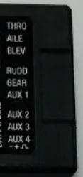
I need part of a RC receiver Model JR R921X 9Ch:
this video shows the receiver: https://www.youtube.com/watch?v=jg3p2cItifw
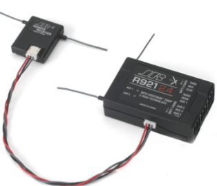
A quick look doesn’t turn up a data sheet with pin outs and positions of the connector. That information is needed to make a part.
Peter
it is similar to the one done above. But they have 9 channels
That should be enough info to make a part. The only jpg I found had the lettering too blurry to use and didn’t have the signal/power/ground connection orientation provided above. I should be able to post a part in a few days.
Peter
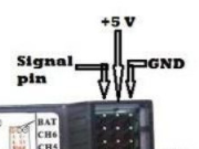
This should do most of what you want. It is missing the two battery (I think) connectors below the servo connectors as I didn’t have pin outs (nor see them til the part was done  .) As well check the servo connections, I set them to the indicator on the bottom of the label (Gnd on top +5V then signal.) The 6 channel pinout is the opposite direction. If you need the battery connections they can be added if you have connector info.
JRPR921X.fzpz (8.1 KB)
Peter
1 Like
peter …man u do amazing job here
Yes. That will do. Thank you for your help
I just built the library of the Flysky R6A receiver. This is the 1st time I made my own library by myself. ![]()
![]()
![]()
![]()
![]() Please let me know if anything needed to change.
Please let me know if anything needed to change.
fs R6A.fzpz (24.6 KB)
I have one question for @vanepp. If I have multiple GND/VCC pins & I want them interconnected inside the library. How can I do that?
You are missing a breadboard layerId so your part won’t export as an image (from FritzingCheckPart.py)
Error 69: File
‘svg.breadboard.prefix0001_458783fd67e9a30b48340fd440e99683_10_breadboard.svg.bak’
At line 9
Found a drawing element before a layerId (or no layerId)
Error 77: File
‘svg.breadboard.prefix0001_458783fd67e9a30b48340fd440e99683_10_breadboard.svg.bak’
At line 19
terminalId connector0terminal can’t be a g as it won’t work.
and it has the terminalIds defined as groups which won’t work in all cases and disappear when ungrouped (they are also in this case misnamed as connector0terminal— which doesn’t match the fzp file!)
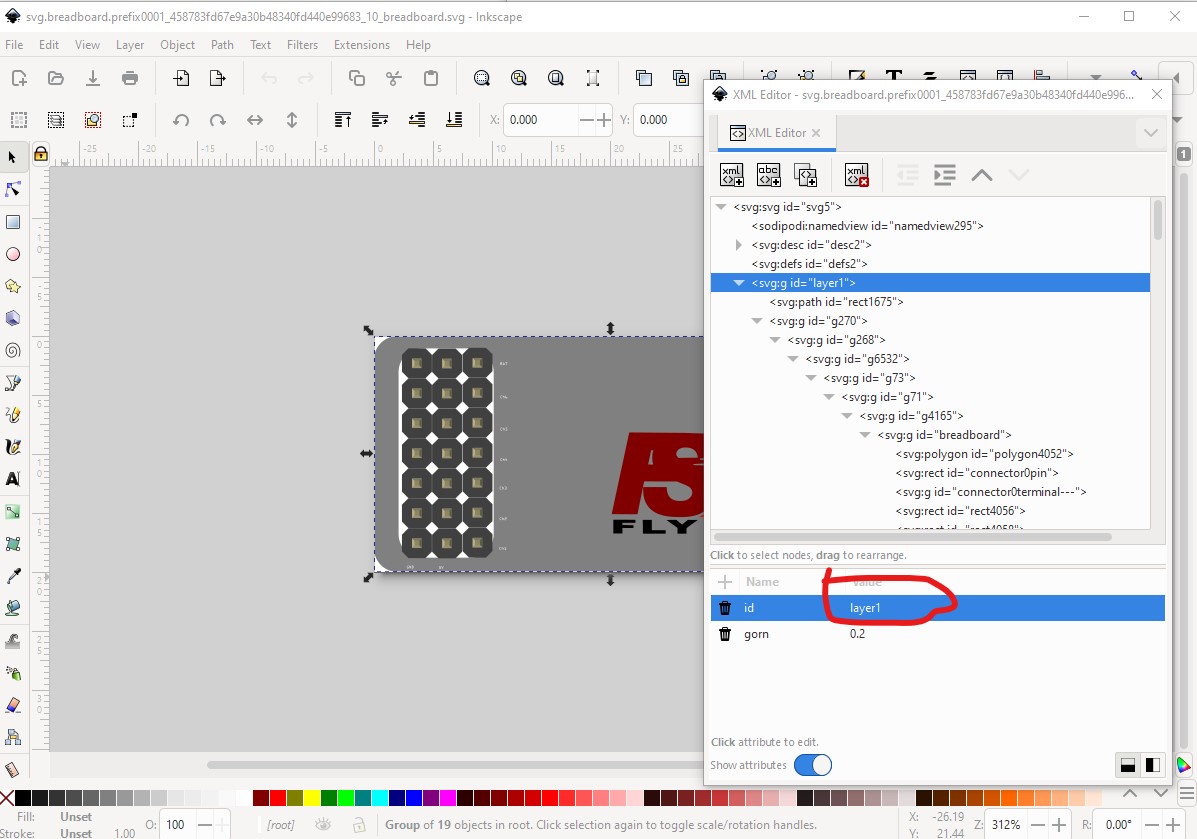
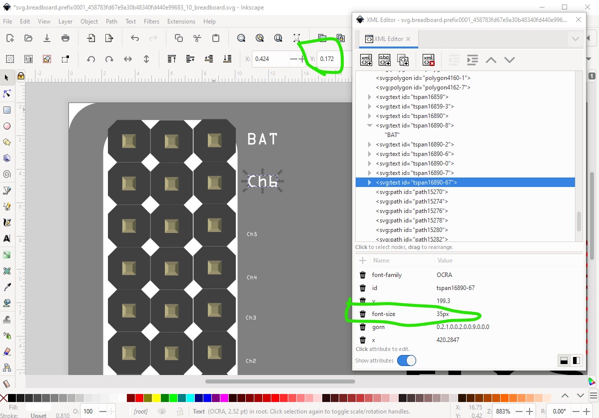
here replacing layer1 with breadboard would fix the layerId error, but instead I chose to ungroup and rescale breadboard to get to the correct scale where 1 drawing unit is 1/1000 of an inch like this
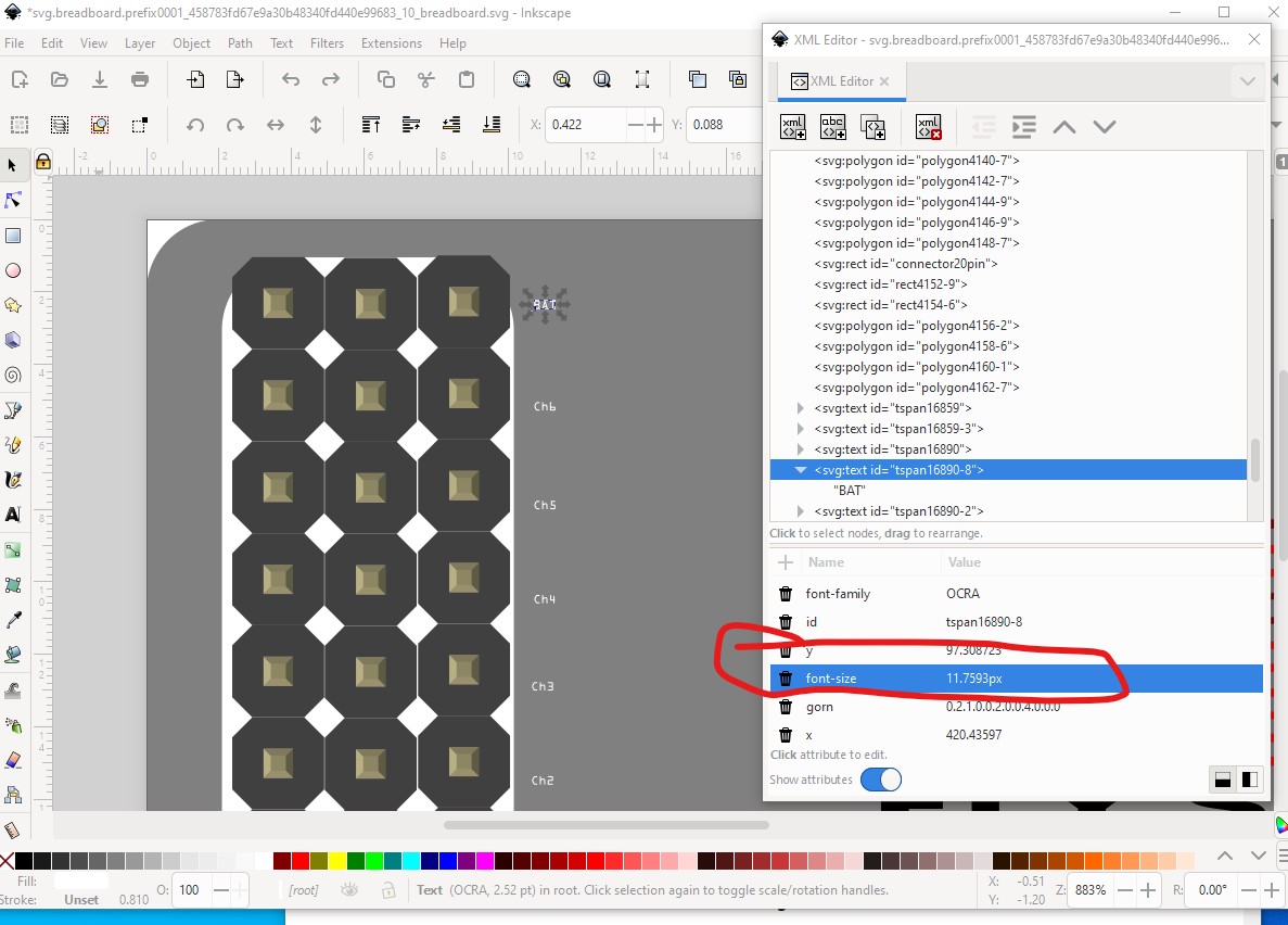
where the terminalIds have no disappeared (because they were a group which was removed) and we can now set the font size to a more suitable value (I chose 35px here and adjusted the y coord to be a multiple of 72 to align the text to the center of the pin)
after doing all the text I then did an Edit->Select All then Object->geoup and set the group id to breadboard then File-> Save as as plain svg to save the new breadboard svg.
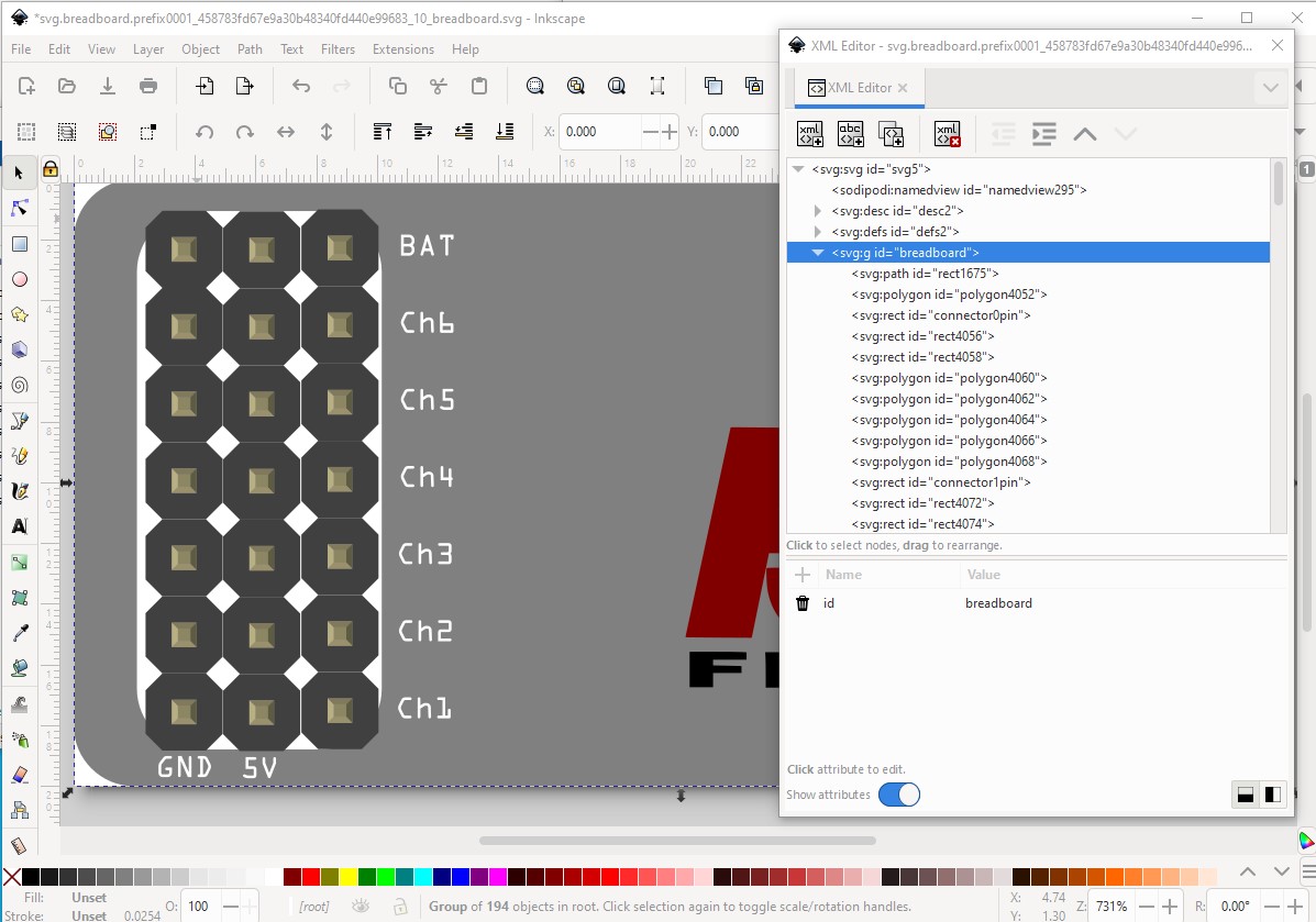
Now on to schematic. While yours will work, a better one can be made fairly easily with Randy’s Inkscape extension but to do that we need to go back to breadboard and change the pin numbering like this:
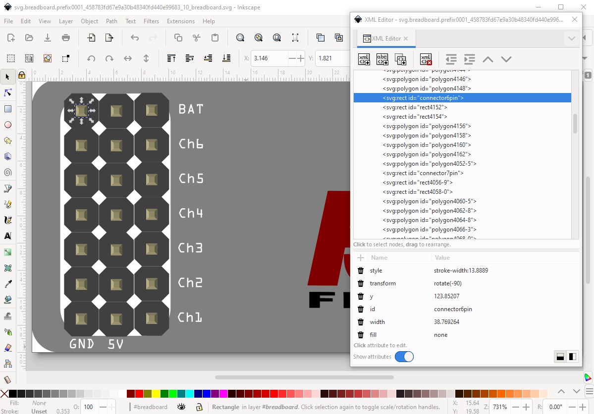
pin6 wants to become pin0, pin 13 wants to become pin1 and pin 20 wants to become pin2. So here I moved them in that order to the bottom of the svg (because I have a script that will renumber them from there!) like this:
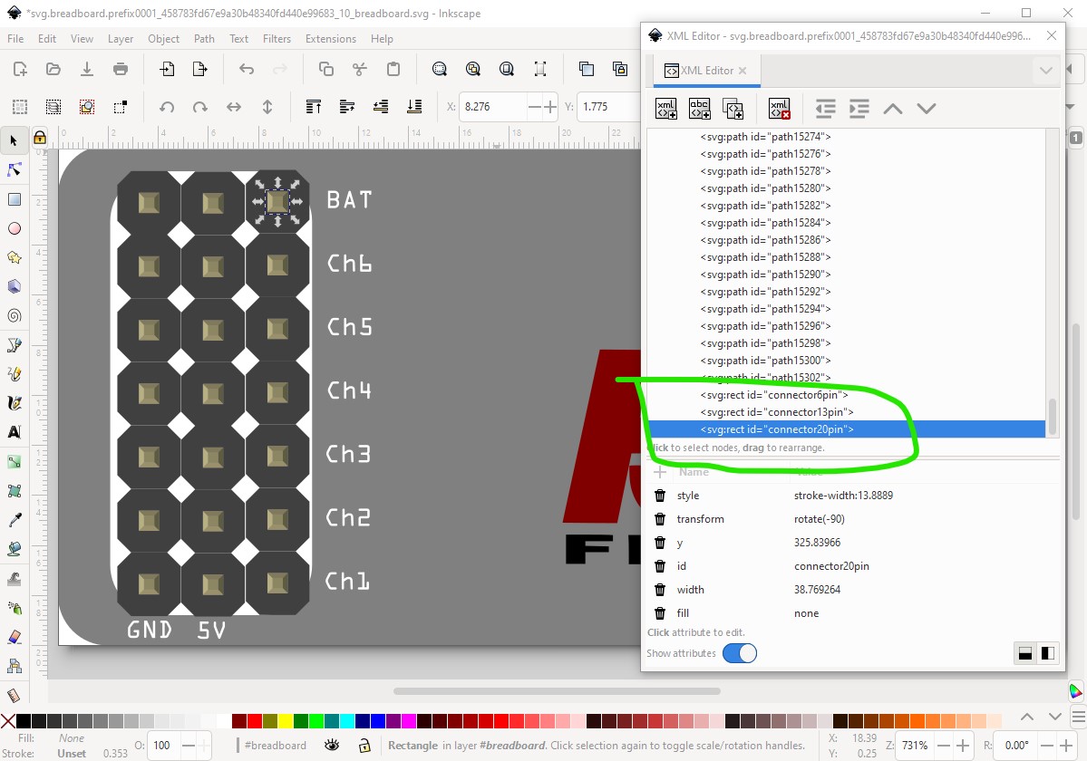
to end up with this
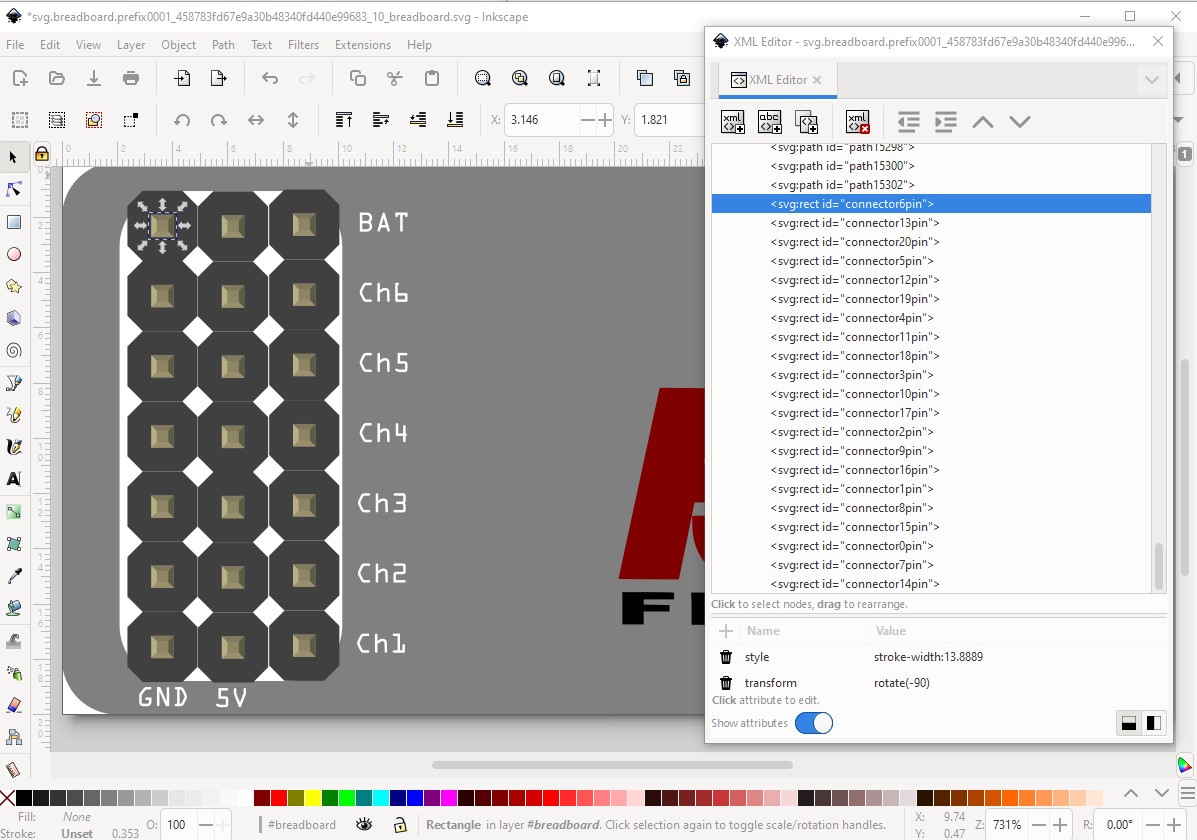
Now I set pin 6 to connector0pin and run my script
$ setbb.py svg.breadboard.prefix0001_458783fd67e9a30b48340fd440e99683_10_breadboard.svg
*** Process svg.breadboard.prefix0001_458783fd67e9a30b48340fd440e99683_10_breadboard.svg ***
and it renumbers the pins in order like this
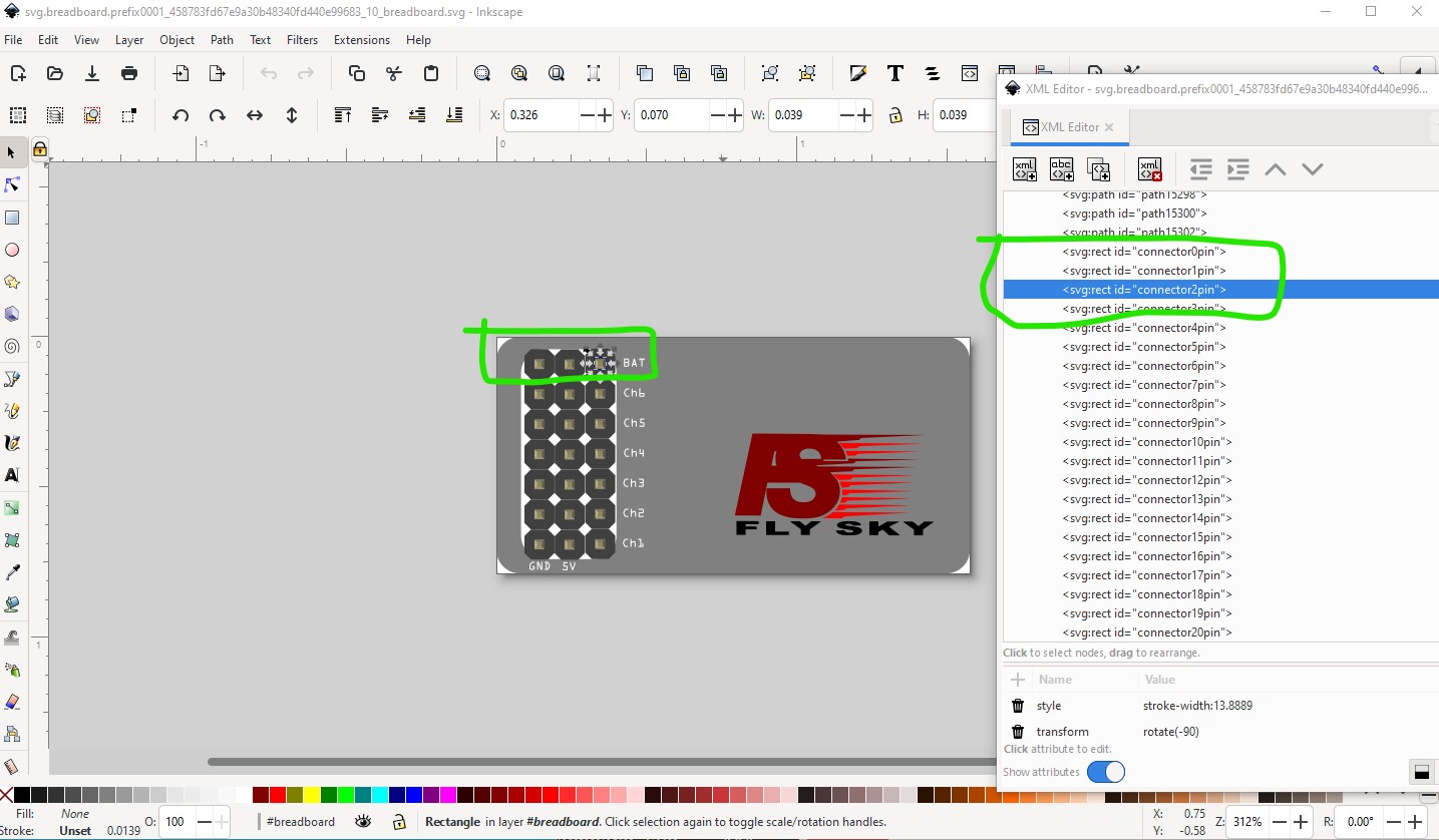
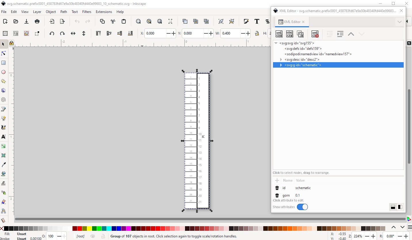
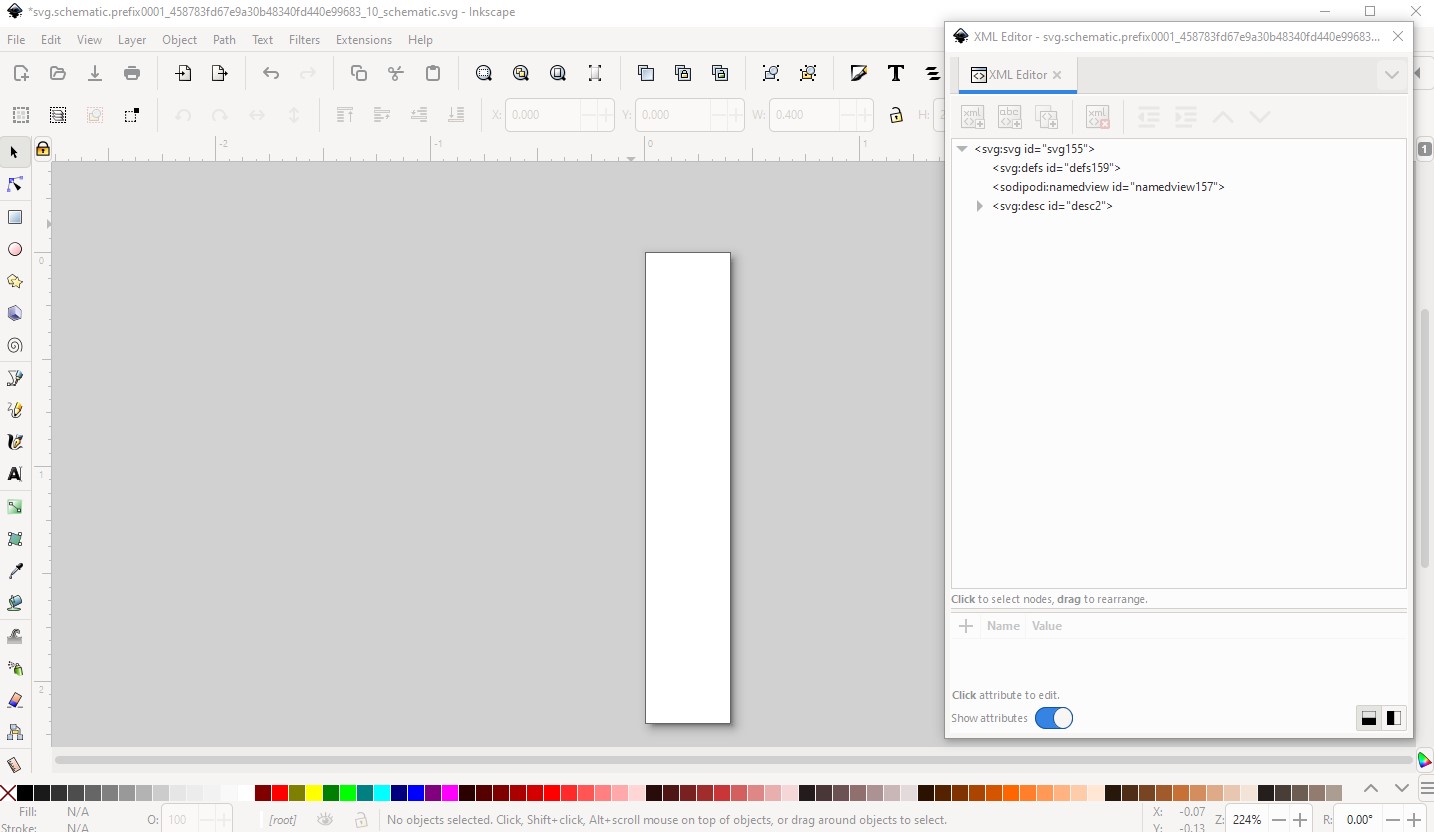
unfortunately until I can clean the script up enough to release you would need to manually renumber the pins in your svg editor to match the above order. Then in Inkscape I start from your schematic (which as noted will work but doesn’t look very good) and delete it.
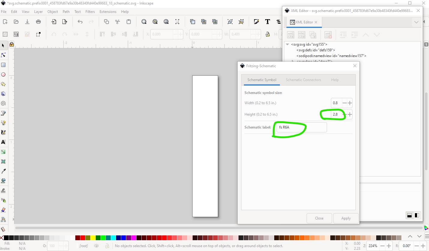
then run the schematic extension then set the Schematic label to fs R6A and the height to 2.8in (2.1in for the pins and .7 for space between each 3 pins if I’m lucky!) and 0.8in wide.
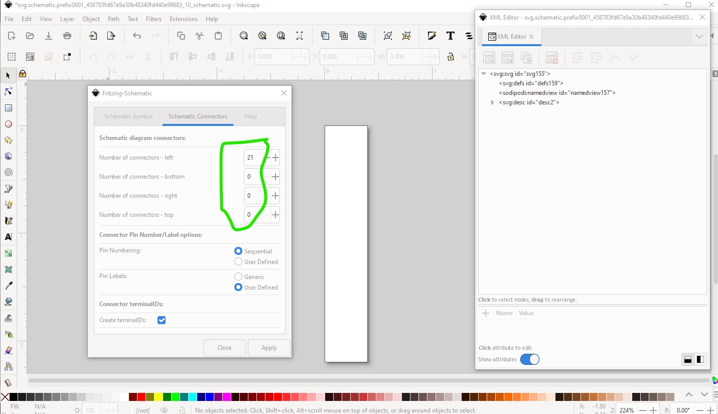
then I set 21 pins on the left side
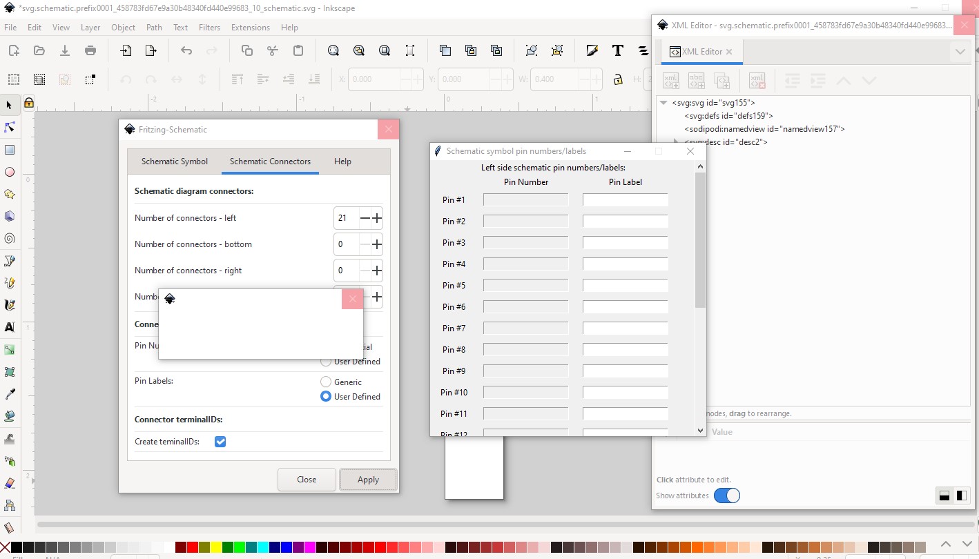
then hit apply which brings up the pin name dialog box.
Now I set the pin names starting with pin 0 like this
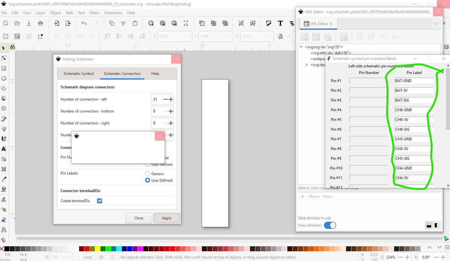
and continue until all pins are done like this
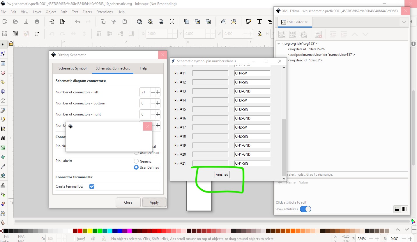
then click finished and close to end the extension which produces the required schematic
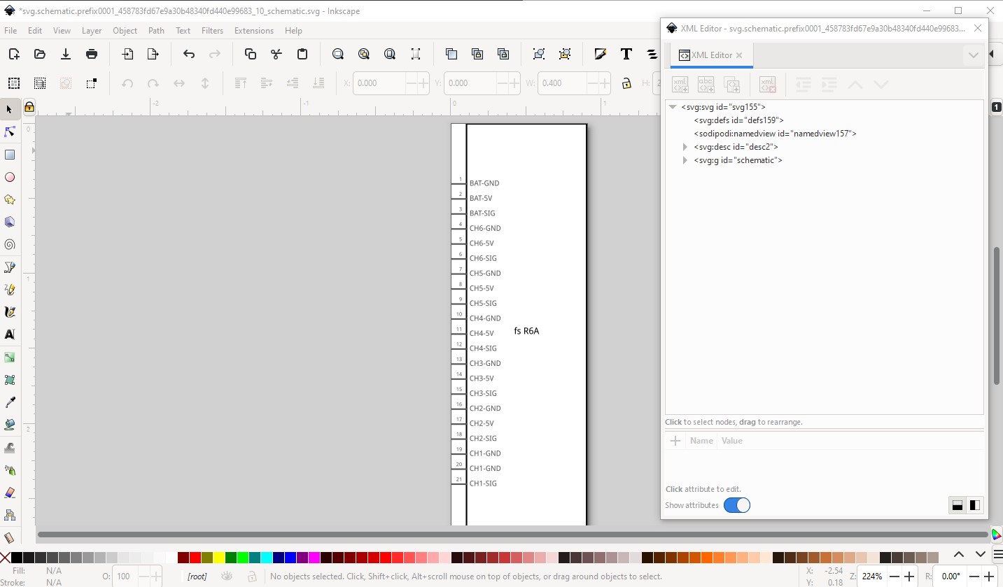
In this case I need to ungroup the schematic to make changes like this
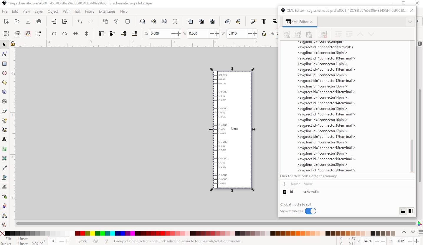
unusually for me I got my math correct and schematic worked out first time! I usually have to do this a couple of times to get it right. Here each servo position is ready to accept a servo connected to it in breadboard and it will connect correctly in schematic (I hope!) So now we have a new breadboard and schematic but with completely new pin numbering. So now we need to edit the fzp file to match what we have done (and to suppress pcb which isn’t useful in this case!) While we do that we will address your question about internal connections in parts editor (which as you see I don’t use) aka buses in the fzp file. Because I renumbered the pins I need to replace the connectors section of your fzp file with a new one generated from this script (which is publicly available here on github)
first I delete all the connectors defined from this:
<connectors>
  <connector name="pin1" type="male" id="connector0">
    <description>pin 1</description>
    <views>
      <breadboardView>
        <p svgId="connector0pin" terminalId="connector0terminal" layer="breadboard"/>
      </breadboardView>
      <schematicView>
        <p svgId="connector0pin" terminalId="connector0terminal" layer="schematic"/>
      </schematicView>
      <pcbView>
        <p svgId="connector0pin" layer="copper0"/>
        <p svgId="connector0pin" layer="copper1"/>
      </pcbView>
    </views>
  </connector>
     ...
      <p svgId="connector19pin" layer="copper1"/>
    </pcbView>
  </views>
</connector>
<connector name="pin21" type="male" id="connector20">
  <description>pin 21</description>
  <views>
    <breadboardView>
      <p svgId="connector20pin" terminalId="connector20terminal" layer="breadboard"/>
    </breadboardView>
    <schematicView>
      <p svgId="connector20pin" terminalId="connector20terminal" layer="schematic"/>
    </schematicView>
    <pcbView>
      <p svgId="connector20pin" layer="copper0"/>
      <p svgId="connector20pin" layer="copper1"/>
    </pcbView>
  </views>
</connector>
to this
  </views>
  <connectors>
  </connectors>
</module>
then
$ cons.py -n -p t 21
to generate a file t with no pcb layer and name as the pin number which then gets copied in to the fzp file like this
<connectors>
  <connector id="connector0" type="male" name="Pin 1">
    <description></description>
    <views>
      <breadboardView>
        <p svgId="connector0pin" layer="breadboard"/>
      </breadboardView>
      <schematicView>
        <p svgId="connector0pin" layer="schematic" terminalId="connector0terminal"/>
      </schematicView>
    </views>
  </connector>
  <connector id="connector1" type="male" name="Pin 2">
    <description></description>
    <views>
      <breadboardView>
        <p svgId="connector1pin" layer="breadboard"/>
      </breadboardView>
      <schematicView>
        <p svgId="connector1pin" layer="schematic" terminalId="connector1terminal"/>
      </schematicView>
  ...
ready to have the description field added with the names defined in schematic like this
<connectors>
  <connector id="connector0" type="male" name="Pin 1">
    <description>BAT-GND</description>
    <views>
      <breadboardView>
        <p svgId="connector0pin" layer="breadboard"/>
      </breadboardView>
      <schematicView>
        <p svgId="connector0pin" layer="schematic" terminalId="connector0terminal"/>
      </schematicView>
    </views>
  </connector>
  <connector id="connector1" type="male" name="Pin 2">
    <description>BAT-5V</description>
    <views>
      <breadboardView>
        <p svgId="connector1pin" layer="breadboard"/>
      </breadboardView>
      <schematicView>
with that done we move on to the buses (which create the internal connections on gnd and 5V you want) like this. Currently it is
  </connectors>
</module>
that needs to change to
  </connectors>
  <buses>
   <bus id="gnd">
     <nodeMember connectorId="connector0"/>
     <nodeMember connectorId="connector3"/>
        <nodeMember connectorId="connector6"/>
      <nodeMember connectorId="connector9"/>
      <nodeMember connectorId="connector12"/>
      <nodeMember connectorId="connector15"/>
      <nodeMember connectorId="connector18"/>
   </bus>
  <bus id="5V">
   <nodeMember connectorId="connector1"/>
   <nodeMember connectorId="connector4"/>
   <nodeMember connectorId="connector7"/>
   <nodeMember connectorId="connector10"/>
   <nodeMember connectorId="connector13"/>
   <nodeMember connectorId="connector16"/>
   <nodeMember connectorId="connector19"/>
  </bus>
 </buses>
</module>
I made some other changes to the fzp file (which you can see by unzipping the fzpz file and editing the fzp file.) as Fritzing will make changes to your part via the parts factory as it stands (which isn’t correct!) as well. All of that (and a run through FritzingCheckPart.py to clean up and check for errors) creates this new file (you will need to delete your old file to load this one as I didn’t change the moduleId or file names!)
fs-R6A-fixed.fzpz (13.9 KB)
Hope this helps. All things done here are available in this tutorial
Peter
This is a completer troubleshooting. thanks. Actually, I am learning. I never built a library in fritzing before. But I don’t see any PCB traces
That is because I suppressed pcb in the original part as this won’t fit on a pcb. I assume you want the connectors to connect to the receiver via a cable which this part will do.
fs-R6A-fixed-with-pcb.fzpz (14.0 KB)
Normally this wouldn’t be useful because you can’t route traces to the middle row of connectors. In this case the first and middle row are all connected together so that won’t matter.
Peter