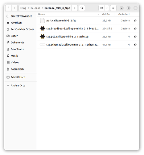
While I can’t access the svg in Calliope_mini_3_PCB_2_i.svg, it won’t render in Firefox, and won’t appear on a right click to save the svg (probably because the svg hasn’t been loaded!) That said I expect the problem is that the .fzp file needs to change to add back in the pcb definitions and Parts editor can’t do that. I took your Calliope_mini_3_V_1.fzpz post and made the necessary changes there (and will explain them here!) to make this new part. I replace the header connectors in pcb with circles sized for 0.1in headers (0.038in) and replaced the paths for the larger circles with circles because Fritzing gerber processing has troubles with paths in pcb usually to create this new part:
Calliope_mini_3_V_2.fzpz (44.6 KB)
As well here is my test sketch which the following images are from:
Calliope_mini_3_V_2.fzz (67.3 KB)
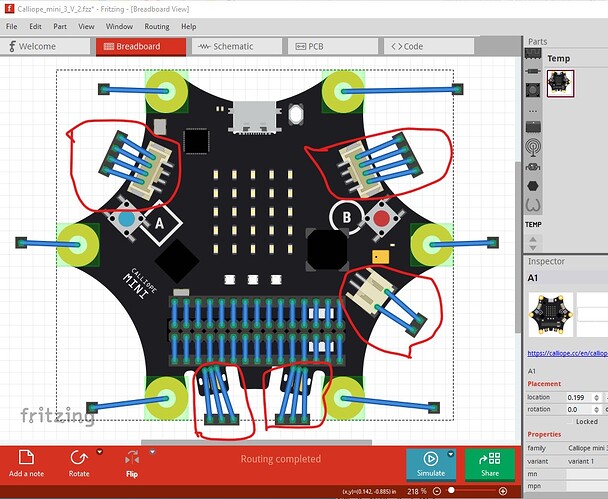
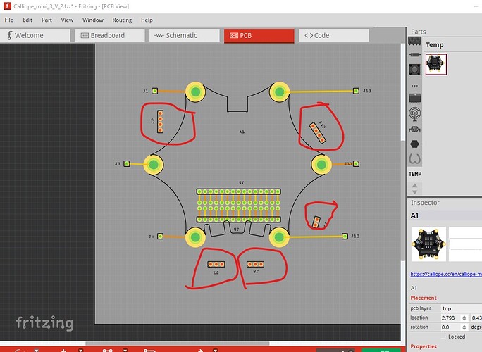
breadboard and schematic don’t change, but pcb now exists except the various connectors are disabled in pcb like this
the connectors that are suppressed in pcb are circled in red here
in pcb the header exists, but there is no connector on the Calliope and no connection from the header.
That needed to happen in the .fzp file (which as noted the parts editor AFAIK can’t change) is this
original here the pcb definition has been replaced with the breadboard svg to suppress pcb view (Fritzing needs a renderer in pcb or it is unhappy, but will use but not display the breadboard svg!)
      <layers image="schematic/calliope-mini-3_1_schematic.svg">
        <layer layerId="schematic"/>
      </layers>
    </schematicView>
    <pcbView>
      <layers image="breadboard/calliope mini-3_1_breadboard.svg">
        <layer layerId="breadboard"/>
      </layers>
    </pcbView>
In the new part this has been replaced by this (a standard .fzp file!)
    <schematicView>
      <layers image="schematic/calliope-mini-3_2_1_schematic.svg">
        <layer layerId="schematic"/>
      </layers>
    </schematicView>
    <pcbView>
      <layers image="pcb/calliope-mini-3_2_1_pcb.svg">
        <layer layerId="silkscreen"/>
        <layer layerId="copper0"/>
        <layer layerId="copper1"/>
      </layers>
    </pcbView>
Then in the pin definitions I needed to add back in the pcb definitions and only remove them for the pins that don’t appear in pcb (basically the connectors)
original file has no pcb definitions for any of the connectors
  <connectors>
    <connector id="connector0" type="male" name="Pin 1">
      <description>GND</description>
      <views>
        <breadboardView>
          <p svgId="connector0pin" layer="breadboard"/>
        </breadboardView>
        <schematicView>
          <p svgId="connector0pin" layer="schematic" terminalId="connector0terminal"/>
        </schematicView>
      </views>
    </connector>
    <connector id="connector1" type="male" name="Pin 2">
      <description>GND</description>
      <views>
        <breadboardView>
          <p svgId="connector1pin" layer="breadboard"/>
        </breadboardView>
        <schematicView>
          <p svgId="connector1pin" layer="schematic" terminalId="connector1terminal"/>
        </schematicView>
      </views>
    </connector>
the new .fzp file has pcb definitions for the pins that will appear in pcb (connector0) but not for ones that don’t (connector1)
  <connectors>
    <connector id="connector0" type="male" name="Pin 1">
      <description>GND</description>
      <views>
        <breadboardView>
          <p svgId="connector0pin" layer="breadboard"/>
        </breadboardView>
        <schematicView>
          <p svgId="connector0pin" layer="schematic" terminalId="connector0terminal"/>
        </schematicView>
        <pcbView>
          <p svgId="connector0pin" layer="copper0"/>
          <p svgId="connector0pin" layer="copper1"/>
        </pcbView>
      </views>
    </connector>
    <connector id="connector1" type="male" name="Pin 2">
      <description>GND</description>
      <views>
        <breadboardView>
          <p svgId="connector1pin" layer="breadboard"/>
        </breadboardView>
        <schematicView>
          <p svgId="connector1pin" layer="schematic" terminalId="connector1terminal"/>
        </schematicView>
      </views>
    </connector>
So this new part should do what you want and allow a shield to be made that attaches to the edge connectors on the Calliope. You can make a shield template from the pcb svg in this part. Hope this helps, ask if anything is unclear!
edit:
I managed to download the svg file finally. It has a few problems though
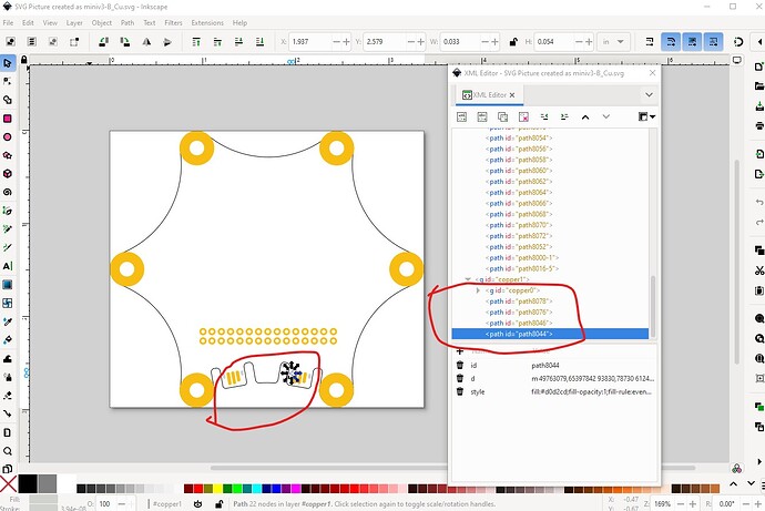
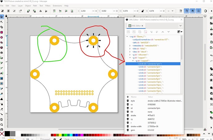
The paths circled in red will appear on the top of the board because they the are in copper1 group but not copper0 (where they would appear on the bottom of the board!) They are also defined as connectors in pcb which is incorrect as they are not through hole. It would be best to delete them all as unneeded like this
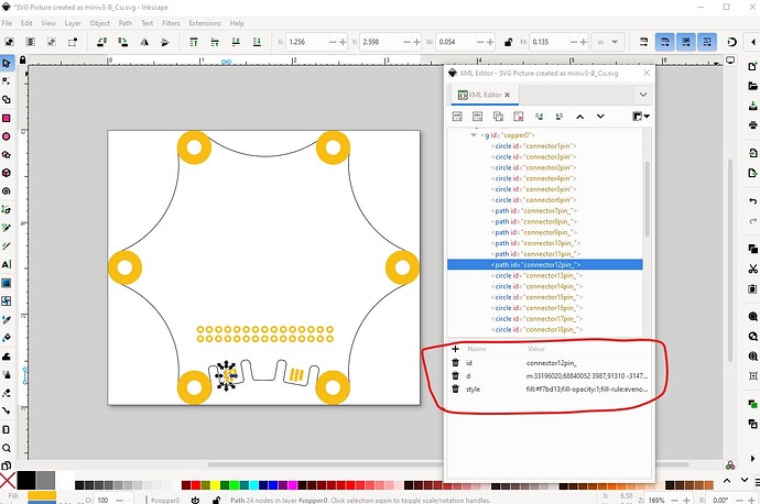
after that the connector numbers need to match the pin definition in the .fzp file. The pad circled in green is defined as connector6pin, but according to the original .fzp file it should be connector0pin, and connector1pin should be the left and down pad not the one on the right. As I said I think the original problem was likely the lack of pcb layer definitions in the .fzp file but incorrect pin numbering will also cause problems.
Peter
