Best way to good PCB fabrication

Hi - I’m getting pretty close to fabrication time for my project. #exciting

As I have explored doing a bit of layout, optimal layout, autorouting, etc, and I’ve got a few concerns that I think I ought to address. But I’m not sure what the priority is for solving these things.

I’ll start with DRC pre-routing - there’s a couple issues who’s answers might provide me insight to what I’m strugging with in the post-routing issues.

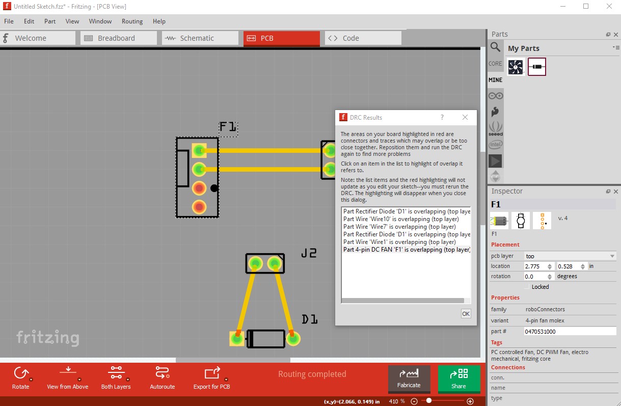
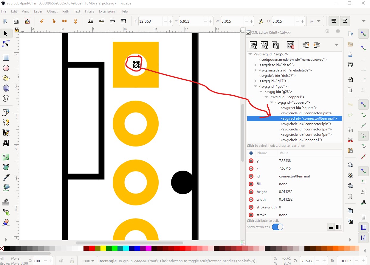
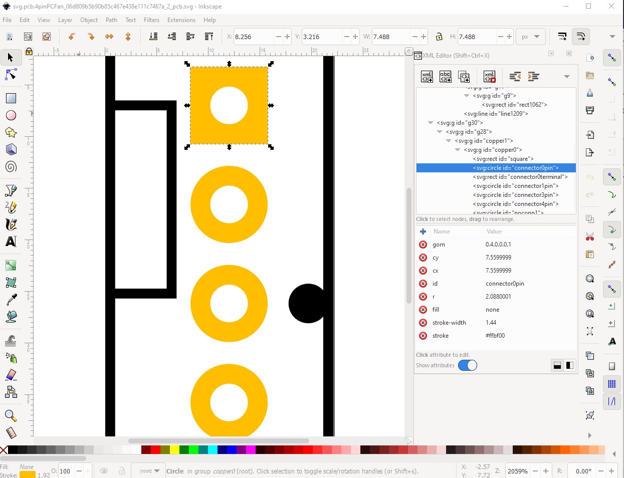
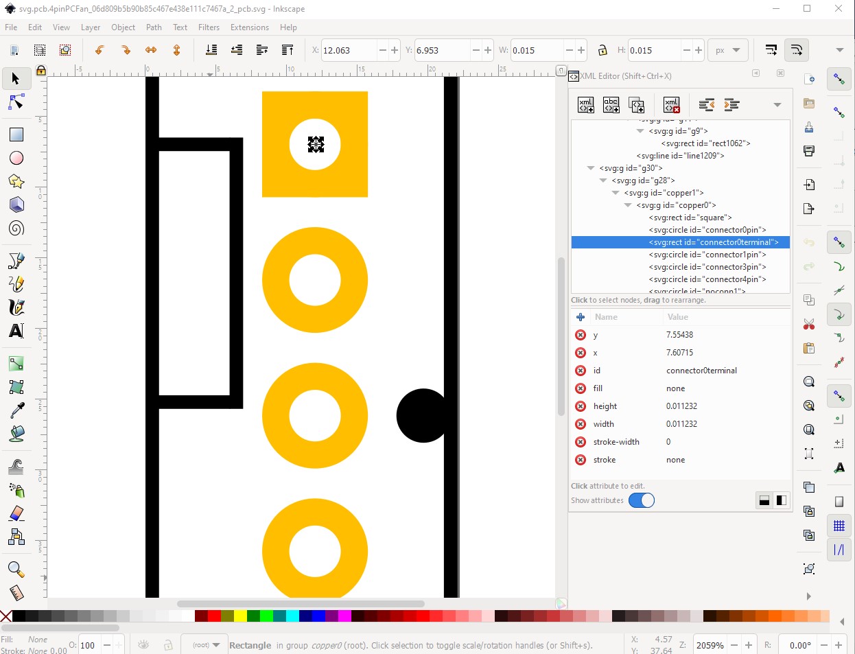
Pre-Route DRC issue 1 - I hand-routed a thick 48mil ground signal a few places and it always runs me into trouble on this particular part. Why do I get (or how do I avoid) this ‘overlapping’ error? Does this have to do with hole size or stroke size on the part? I have been using a 20mil stroke and a circle size of 78mil.

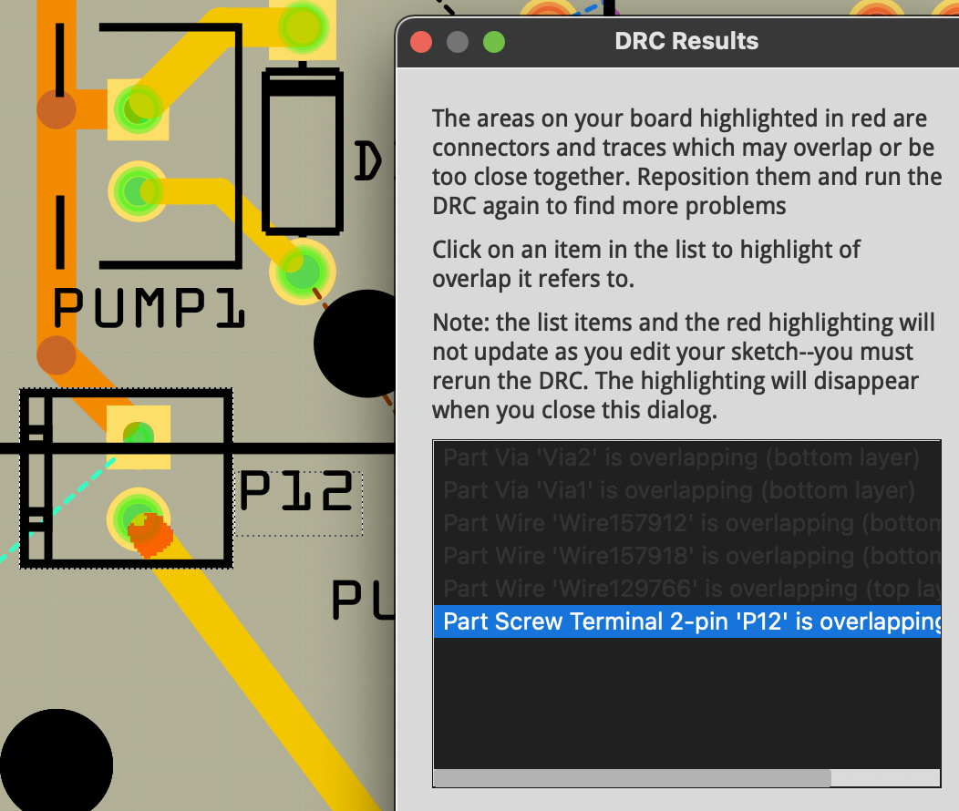
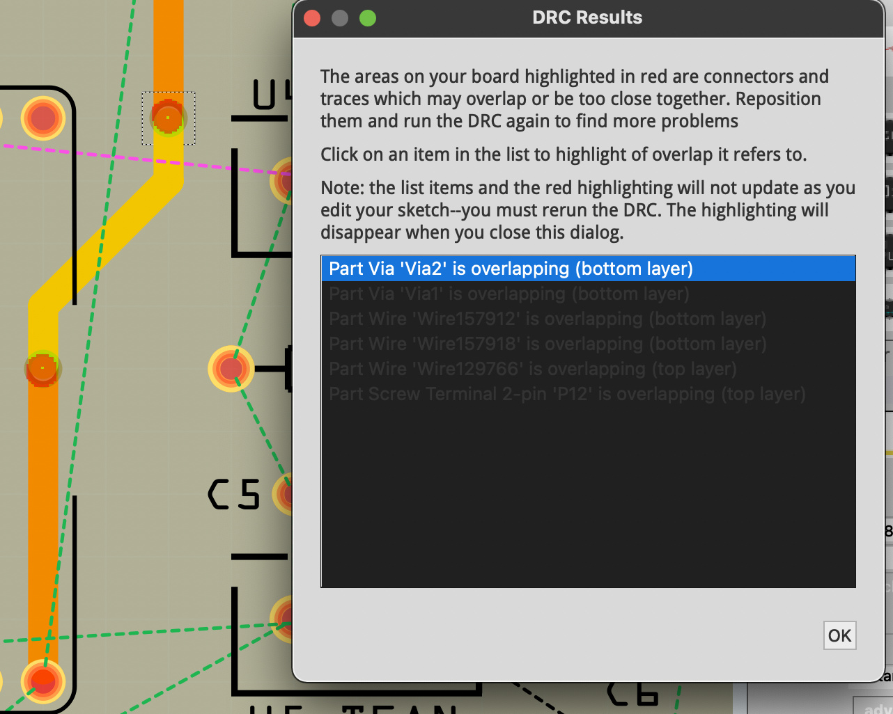
I also hand-routed an inbound 5V signal from its inbound connector to the ESP32 VIN pin and I didn’t want to “block” a large swath of the board from autorouting so I wanted to place a portion of that trace on the bottom layer and a portion on the top. So I made it 48mil thick and placed a standard pair of vias along the way. The pre-route DRC issue #2 is about overlapping at the vias. It actually complains twice for each via - once for the ‘wire’ overlapping on the bottom layer and once for the ‘via’ overlapping on the bottom layer.

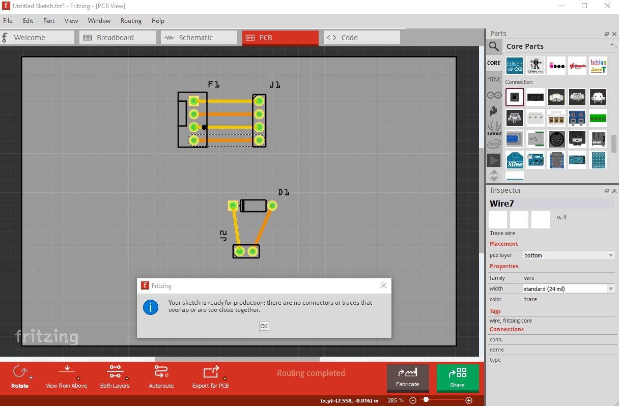
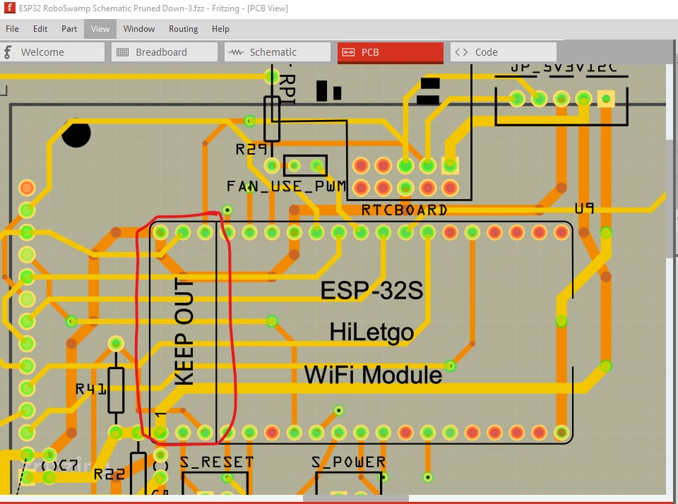
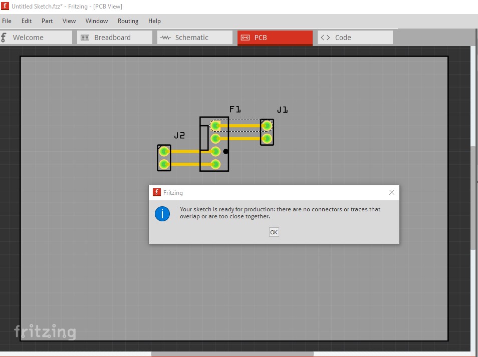
Now, I do an autoroute and I get a successful route. But when I do a post-route DRC, I get a LOT of issues (like 40+). These fall into two categories in my eyes - complaints where it looks like the autorouter routes a trace too close to a part’s hole/copper as seen in post-route DRC-3 issue:

And another, probably related, where the router seems to route its own wires too close to themselves. I don’t have a picture of this but wonder how to fix all of these? Manually?

It seems odd that the autorouter violates the DRC rules that it ought to already know. If I can minimize these issues by changing something. I’d love that.

Thanks,
bob

Well, let me first start off by saying I’m not the most knowledgeable person on this subject.

Anyhow, I don’t think the DRC is very good at what it does. In my most recent project that I had boards made for, I had a number of DRC issues, yet the boards worked fine.

I got over lapping errors for every pin on the ESP32 part, but yet no errors on any other parts. In my case, I assumed it was a problem with the ESP32 part I was using. Every single part I used had solder pads on the top and bottom of the pcb, but only the ESP32 produced that error. Much like your via error.

Yea, as I just mentioned, I don’t think you have to worry about this one. It’s like the ‘Part Wire is overlapping’ error that is in your screenshot. For me, I got this ‘Part Wire is overlapping’ error message for every trace on one side of the board the crossed over a trace on the other side of the board. However, I’m not saying to ignore these overlapping errors. I did find two traces overlapping on the same side of the board in my project.

That’s a simple one, don’t use autoroute, ever.

Autoroute is one part of the software, DRC is another part of the software. One preforms a task of routing traces, the other preforms the task of checking for errors. The routing part of the code isn’t aware of the Design Rule Checks rules.

Autorouters do a horrible job at what they do, even in the most expensive EDA software package.

Take a look at the last screenshot you posted. The RTC part has two green pins on the top row with traces connected to them. The orange trace appears to be hand routed and is too close to the connector pins of the RTC part. It also has a square 90 degree bend to it. And the next trace over, the yellow one, has an even sharper bend to it. Generally, in PCB design, two 45 degree bends are preferred over a single 90 degree bend.

And I’m sure I missed a few things that I should have mentioned. See the disclaimer at the top of my post…

please feel free to ask questions… and good luck!

Randy

The best bet is to post the sketch (the .fzz file) so we can download it and look at it. It is almost impossible to say what is wrong simply from images of the errors. Sometimes as @just_randy mentioned parts (even some in core parts) are incorrectly configured and cause problems. As long as you are sure that the DRC complaint isn’t valid, you can cut boards and have them work, but I prefer to fix the broken parts so that DRC passes because that is safer.

Peter

Thanks to both of you for your comments. I decided to give up on autorouting and see how far I got before pulling my hair out. Turns out it wasn’t so bad. I used my old adage of having vertical on the back side and horizontal on the front side generally and made my ground and power traces 48mil. Went pretty well. I still wound up with 20 or so DRC check issues with the left side of the board specifically. I am feeling kinda proprietary about the full design file so I think I’ll try pruning it down to just this particular part of the board and upload that for you to take a look if that’s ok. Especially since it seems to be picking on a few parts in particular. Would be super nice having a fully clean DRC check before going to fab if possible. :slight_smile:

Sure, as long as the DRC error occurs we can likely tell you why.

Peter

Awesome well that was easier than I’d figured it would be. Here’s the fzz file. The DRC errors still occur all on the left end of the board.
ESP32 RoboSwamp Schematic Pruned Down.fzz (321.7 KB)

As a related item, I find it curious that the drill file shows so many variations of hole sizes. It would be super slick if the parts library were consolidated down to a single hole size for basic through-hole parts. Here’s the hole sizes from my full design even after trying to consoildate things a bit. I went through and identified by position of the holes which ones were outliers and am still scratching my head why they’re different by small amounts. T1 is from the Molex Fan connector locator hole and T2 is a mounting hole at 40mils. T100+ are the plated holes ranging from 27.28 mils to 40.795 mils.

M48
INCH
T1C0.040000
T2C0.135000
T100C0.038333
T101C0.040333
T102C0.032000
T103C0.038000
T104C0.027280
T105C0.015748
T106C0.038795
T107C0.035000
T108C0.030000
T109C0.040795

A quick first look shows that you have several custom parts in that sketch. Is there a reason for (example) using a roboswamp specific version of a basic diode, instead of the one from core? The reason to pick on that case, is that I see that it is involved in several of DRC collision reports. The square pad for the diode was created using a rect element at the same position as the circle. That specifies stroke="none", but it might still “cover” the drill hole. Replacing D1 and D2 with the core diode (using delete minus) got rid of those reports from DRC. It would take more time to narrow down exactly what is wrong with the custom diode part. I tried copying (exporting) that part, removing the rect element, recreating the diode (with a new module id), and replacing one of the original diodes with my copy. That still got drc errors, so it is not ‘just’ the rect element causing the problems.

Whatever the root problem, it is likely the same thing in other custom parts in the sketch. 2 more cases that are being reported are the square pads for FAN1 and FAN2. The final case is the round pad for P12.

If that rect element with stroke and no fill is actually valid, it is much simpler than the filled path element that I (and others) have been using to get the same effect.

Two of your custom parts are misconfigured, the diode and the fan (I didn’t check further …) The diode started out as a bendable leg part although that likely isn’t the cause of the problem since DRC doesn’t care about bendable legs AFAIK. I don’t see anything obviously wrong in the pcb svg, but rescaling it and cleaning up a few things makes DRC happy. First with your original parts:

both report DRC errors. With my two modified parts DRC passes.

and the modified parts

4-pin DC FAN.fzpz (115.6 KB)

edit: uploaded the original part, not the fixed one. Reuploaded the correct part.

Rectifier Diode.fzpz (5.5 KB)

The radius in the pcb svg files was varying a bit from floating point round off. The radius (after rescaling) was 29.0008 rather than 29 as it is in my parts which will cause a slight hole size difference. Here is the gerber drill.txt file for my fan and diode:

; NON-PLATED HOLES START AT T1
; THROUGH (PLATED) HOLES START AT T100
M48
INCH
T100C0.038000
%
T100
X018222Y015777
X017722Y007277
X018222Y018777
X013222Y015777
X018222Y017777
X013222Y016777
X016722Y007277
X013222Y017777
X013222Y018777
X016222Y010777
X018222Y016777
X019222Y010777
T00
M30

edit: an unrelated to this problem point: the keepout area (circled in red here) is meant to have no traces running through it. They tend to short tha antenna causing radio problems. That may be just this cut down example though …

Peter

Hey all,
Thanks for the interaction here. I’d LOVE to nail down these mysteries for myself and others.

@microMerlin - I actually only modified the diode from the parts library because i had a suspicion that larger hole sizes was frustrating the DRC or autorouting process. So my modified version was intended to clean up hole size - and I found that it did not solve the issue. Oddly enough, when I go back to the original parts library version, I still get DRC issues on one of the pins.

@vanepp - a few things…

  • Thanks for the revisions. This is helpful in doing a ‘diff’ between .svg files.
  • The diode you uploaded I think is your non-modified one from me. a) I dont see a difference in the files. b) If I edit my part and do a ‘load’ of your svg.pcb.* file from inside the .fzp file to effectively update my part, I get no difference in DRC.
  • Your Molex fan connector DOES work for me in terms of DRC correction. Interesting. Let’s explore this so I can ground out on what I’m doing wrong in creating parts, please.
  • The Molex part has a non-plated through-hole which I had in the copper layers as a 40 mil dia hole. You moved it to the silkscreen. Is that the correct location for it? And related … while it got moved, it disappeared and got relocated it seems. I’m happy to take a corrected version from you with the through-hole corrected or to create the version myself when I figure out the scaling issue that I think is the root of all evil for me. :slight_smile:
  • Your non-related note about the keep-out zone - my project is not using the radio and so my belief is that I don’t care about the keep-out zone. If someone knows of ill effects to my traces from the antenna that would be problematic, I’m up for hearing about it but my thinking is that the radio is off so it doesn’t matter to me.

Now - off to Inkscape … when I look at the Molex/Fan connector PCB part, the glaring difference I see is at the top level - something to do with viewport and such. So I went in Inkscape and did a “File -> Document Properties…” and I see the scaling difference of the document clearly. Both documents are set to ‘inches’.

As you can see, my incorrect version shows a scale of 72 which is probably related to 72dpi (screen resolution) while yours shows 1000 which is conveniently the number that gets you inches in “mils”.

Ok so I ran with this and took my version and changed the scale to 1000 hoping to see all of my cx and cy values change as well as my ‘r’ values turn into “20” for a 40-mil diameter or 20mil stroke. NOPE. Didn’t happen. GAH. It seems I’m missing something in how to ‘rescale and clean up’ as you put it. Please enlighten me!

I’d like to get down to a set of PCB rules and process that yields good results and am happy to iterate on this until we nail it.

Oh - also I did notice that my XML has transform/translate and I know this to be a “no no” so I did also remove that from my version in hopes that things would magically scale but they didn’t. My translate was just an offset so no biggie. But I tried it as a fix.

bob

I have (but not released yet because it may yet change with the new version of FritzingCheckPart) a version of PP.py that sorts the attributes. That means you can successfully diff svgs from older versions of Inkscape which output the xml in random order. I think Inkscape 1.0.2 already does this but the 0.9 series did not.

Yes, I just replaced it with the correct one.

This is on my todo list so FritzingCheckPart can bitch about it as an error. I suppose I can move that to the top of the list and figure out what is actually wrong now.

I’ll have another look at the part in a bit. Yes, general practice is to put mounting holes on silkscreen rather than drill the hole. The reasoning is you can drag a hole from core parts/pcb in to the sketch if you want the mounting hole (place and size the hole to match the hole in silkscreen), but if it is in the part you have to modify the part to delete it if you don’t want the mounting hole. Either way will work, the silkscreen method is preferred.

That should be correct. If you aren’t using the radio then you don’t care. Wires through the antenna won’t damage anything but will degrade the sensitivity of the antenna by modifying is pattern.

It is a little more complex than that. It is detailed here (with one not yet made modification)

The modification that I need to add to this document is that you also need to lock width to height in the tool bar. If you don’t do that circles get turned to ellipses due to floating point roundoff. With width locked to height they remain circles which cuts down the pain a whole lot.

While I still prefer to remove transforms (because they sometimes cause problems) and I thought that they should be an expensive operation, Kjell says profiling Fritzing indicates transforms aren’t a performance issue and sometimes they are unavoidable. There are cases such as a transform in copper0 that isn’t in copper1 that FritzingCheckPart will flag as an error because it breaks things, but other than that they should be OK. I will go and look/experiment to see exactly what the issue between the working and not working parts is.

Peter

The fan is fairly easy. There shouldn’t be a terminalId in pcb typically, and in this case it causes the overlap. FritzingCheckPart actually flagged this, I just ignored it (then deleted it as uneeded)

Error 74: File
‘svg.pcb.4pinPCFan_06d809b5b90b85c467e438e111c7467a_2_pcb.svg.bak’
At line 36

Connector connector0terminal has no radius no hole will be generated

The message isn’t as clear as it might be, but it is there. It is actually complaining about the lack of a hole not the overlap as well.

Remove that and remake the part (avoiding running a trace across the hole for the pin which will also cause a DRC error) and the original part now works.

4-pin DC FAN-noterm.fzpz (115.7 KB)

Now on to the diode.

Peter

Peter,
Thanks, as always, for your work and detailed docs.

  • I tried the re-uploaded diode and it works like a champ. I’d still like to better understand WHY. I’ll read the (long) post you referenced as that is going to cover the scaling question, or so it sounds.
  • The Molex/Fan connector - my svg for that part does not have a connector0terminal. I think that got introduced in your experiments at some stage. My original and the version you uploaded both do not contain this item. I did, however, notice that instead of having connector0pin through connector3pin, yours had connector0pin, connector1pin, (skip 2), connector3pin, and connector4pin.

Now the 2-pin screw terminal “P12” is the last one that needs corrected and I’m hopeful as I read your post on “how to” that I’ll discover the secret sauce I’m missing and get a correct part with no DRC complaints.

–bob

OOH - and a question I keep forgetting to ask – inside of the realm of PCB xml/svg files, should the id inside copper1/copper0 be *pad or *pin? I thought I had read or been instructed in a video that PCB items should be id=“connector0pad” rather than id=“connector0pin” but I’m not certain.

I’ll have to check again but I believe that is in the .fzz file you uploaded. I exported the part from that file. I knew it shouldn’t be there in the corrected part and deleted it.

That is a common output from parts editor (and I don’t use parts editor …)

Either will work as long as the fzp file matches but the usual convention is pin for through hole and pad for SMD.
I’m still poking at the diode, I so far haven’t seen where the problem is. I may have to look further than the pcb svg although I don’t think anything from breadboard should affect pcb. I’ll look over the 2-pin screw terminal “P12” after I figure out the diodes actual problem.

Peter

Ok - getting closer to healthy. Thanks for the answers - the pad vs pin bit makes total sense and will stick with me now that I realize why I saw some tutorial saying “pad” instead.

I fiddled with the 2pin Screw terminal (P12) and played the re-scaling re-sizing games in your link and while it was VERY contorted and not a very fun experience, I think I did wind up with a healthy part that worked in my pruned down test vehicle.

The following .svg is what I imported and the DRC passed! (this is a zipped .svg file masquerading as a fz file as I couldn’t get svg or a renamed svg->fzp to upload)
good_2pin.fz (1.0 KB)

OK, took me a while but I have solved the mystery. Fritzing is objecting to this xml

    </g>
<g  partID="856998370" gorn="0.4" id="copper1">
    <g  gorn="0.4.0" id="copper0">

specifically the partID=“856998370” if I take that out the DRC errors go away. Same on the diode which has a similar line. As to the fan, here I loaded your ESP32 RoboSwamp Schematic Pruned Down.fzz in to Fritzing then right clicked and export on the fan part and unzipped the .fzpz file. That gets me this in pcb:

so far so good all looks clean. But selecting one element down in xml editor finds

a terminalId in the center of the circle on connector0pin which is what is causing the DRC error. I expect given the pin misnumbering that this file got edited in parts editor and for some reason it decided to put a terminalId in pcb and do its usual skip a number on the pins. I’ll add a check for terminalId in pcb to FritzingCheckPart which should catch this particular problem in future. I don’t know where the partId field came from, I’ve never seen it before (but that doesn’t mean much either, there are lots of things in Fritzing I haven’t seen before :slight_smile: .)

Peter

I have seen “partId” attributes in exported svg images. It is used to help differentiate between multiple copies of a part in a sketch. My guess would be that some where/when, an export was done, and the svg from that edited to create a file for a new part.

I described in the forum before another way to do the rescale to mils. This time, I formalized that a bit more, and dropped a document on the wiki. This version uses manual editing to create a scaling wrapper element, then uses Inkscape to ungroup to apply it everywhere. It avoids all of the convolutions that using Inkscape by itself needs to get the scaling right. As long as you are comfortable using a text editor on an svg file.

Rescale pixel size in svg image

@vanepp - It would appear I haven’t seen the ‘terminal’ issue since my workflow is kinda reverse of yours. I only import/load my svg when I want to update the part (fan or diode) and so these issues I haven’t seen.

I was able to do the rescaling successfully so I wound up with a clean DRC and submitted for fabrication. PHEW. Did a full redline effort this afternoon and actually found an issue with the ESP32 part NOT having one of its grounds attached to ground. It would seem maybe the part has an internal bus and so I wound up without any remaining ratsnests. But when I redlined it I wound up with a pin that was not mentioned (not connected) and so I was able to catch it. Yeah for details.

@microMerlin - thanks for your input too. I’ve given a quick read of your method with scaling by 13.8888x and that’s interesting too. I’d love to see some of this stuff automated. It’s way way too complex and error prone currently.

The end result is a gorgeous 2-layer board with full ground-fill and I’m quite hopeful it’ll work first go. But the parts process is too weak and tedious. Even if we didn’t solve all of the custom part issues, maybe we could solve 90% of the issues with a smaller work effort/solution.

bob