Befuddled by the terminology and lost in the technology!

This is a hi and help plea from a total novice to everyone that can assist please.
Yes Vanepp, I think that you are about to read a post from someone that’s even more of a novice than you were!
I’m in the process of trying to make a VERY simple pcb with 2 off 8 pin relays, 2 diodes, a capacitor, 5 off input wire connectors and 10 off output wire connectors!
I initially played with the Fritzing programme to see how easy it was to use and created a pcb and schematic that appeared to work using the parts already in the parts bin.
Now I want to make the same using the correct size relay pin spacing and connectors that I can use for “flying leads” to create a pcb I can use, but I’m not making any progress fast!

There are questions like what size is a “mil” for pin spacing and why can’t I edit an 8 pin relay for my own purposes etc?
I’ve tried to create the relay in Inkscape, but can’t open it in Fritzing and don’t have the computer skills to fathom out how to do it either.
I’ve read through some of your posts looking for assistance, but get totally confused with the terminology you all use.
This is where I’m at now really.
Attached is my initial try but I now need to create one that can take the relay that I want to use, which is an OMRON G2R-2 type 8 pin relay.

AntiStress Box2.fzz (24.6 KB)
AntiStress Box2_pcb

Any assistance that you can provide would be very appreciated.

Cheers,

Rich

To be fair I had been using EDA programs for more than 30 years before coming to Fritzing so novice only applied to Fritzing :slight_smile: but Fritzing is still a challange even then.

The first is easy: a mil is generally a thousandth of an inch. The second is less so because you can’t actually do that without making a new part and there doesn’t appear to be a part for the OMRON G2R-2 yet (although I remember a couple of other omron relay parts from the past they were G5R). We would need the exact model of the relay you want to use to get the pin out and contacts and from there we can create a part for it. Creating a part is fairly easy once you learn how but the learning curve is steep.

Peter

Hi
I had a quick look, there are a lot of OMRON G2R-2 variations… so a specific part would help.
If it helps, have a look at the RT424F05 relay, although it is a 9 pin relay the outside 8 pins appear to be the same layout as the 8 pin layout spacing of a lot of OMRON G2R-2 relays.

If you want to know how to make parts.

If it too hard you have to post a link to the datasheet.

Hi Barnys1,
Thanks for taking the time to look at my message and for your reply.
I’ll look at the RT424F05 relay and see if I can use it.

The OMRON G2R-2 is the part number they give, it’s at the top of page 154 in this link:

http://docs-europe.electrocomponents.com/webdocs/1420/0900766b814209a2.pdf

The full listing is:
" Relays with PCB Terminals
DPDT Relays
G2R-2, G2R-2-H"

Cheers,

Rich

Hi Vanepp,
Thanks for looking at my thread and Yes it’s a very steep learning curve, but the most frustrating thing I’m finding is the number of questions one wants to ask seems to increase each time you try and complete a stage…but there’s no one there to guide.
I tried to follow the suggestions given in yours and other peoples posts before starting this thread, but don’t fully understand the information given.
I’ll have another go today.
Thanks again.
Cheers
Rich

Hi Old_Grey,
I already had a look at one of your creating part threads (the one spread over two pages) but didn’t completely follow what you were doing.
Thanks for the link I’ll definitely take a look at this Video Tutorial, maybe by seeing what you’re doing will help to answer the questions I have from my lack of understanding of the subject.
Cheers,
Rich

I have compared the dimensions on the RT424F05 and G2R-2, G2R-2-H datasheets. If you ignore the 9th pin on the RT424F05 it looks like they have the same foot print, they also have the same Common (CO) and Normally Closed (NC) pin layout.
http://datasheet.octopart.com/RT424F05-Tyco-Electronics-datasheet-11089829.pdfdatasheets
In the absence of someone making you a specific part, then the RT424F05 may work.
Have a look at (compare) the two relays on their datasheets, specifically the pin dimensions, pin spacing and each relays overall (outside) dimensions.

There is very little written guidance but we are happy to answer questions here. To that end I modified the RT424F05 part that I posted here earlier to create a part for this relay and kept notes as I went along. You could start with the RT424F05.fzpz part and try and follow the notes and see if you can create the same G2R-2.fzpz I got (and ask if you have problems). Note you can do the none svg editing part of this with Parts editor but it doesn’t tend to work well for me so I edit the underlying files instead.

edit the RT424F05 part in parts editor to change the metadata.

use 7zip to unzip G2R-2.fzpz

Breadboard svg:

In Inkscape

ungrouped everything

remove the 9th pin on the end of the chip, change the chip label (although that will happen automatically)

Renumbered the pins in to standard IC order (the top row was backward) for neatness.

edit select all

resize page to drawing or selection

group (still with select all) and change the id to breadboard.

save as plain svg

Done.

pcb:

In Inkscape

ungroup everything

Renumber the pins to match breadboard

select only the copper pads and group twice (so one group is below the other)

The new group should only have square (for pin 1) and connector0-7pin in it.

set the first group id to copper1

set the group id under copper1 to copper0

select line 7 (the top line in the silk screen in xml editor) and group it

change the resulting group id to silkscreen

now for the other 4 lines select them in xml editor and click Indent node (at the top of the xml editor box)
to add them to group silkscreen one at a time. There is no easy way to make a selection that will do this as far as I know (I’d be happy to be shown to be wrong though!)

Don’t resize the page to drawing in this case because that will add a transform to the coppers and break things.

save as plain svg and done.

Schemtic:

In Inkscape:

ungroup everything (this is painful because there are transforms and the text font sizes are now wrong and need correcting)

It is also scaled wrong so correct that first.

edit select all

resize page to drawing

record the coords in px from the tool bar

x 0 y 0 w 97.016px h 46.879px

edit->preferences->Behaviour->Transforms->Scale Stroke Width needs to be ticked (I usually want it unticked to not screw with
stroke widths when changing the size of lines in a drawing)

in document properties change scale from .75 to 10.41667 (why not 10 I don’t know, but this scales properly to 1px = 1thou in maybe because of 96px per inch?)

then click the drawing to make it take effect.

The image shrinks to the top left corner

now edit->select all

and change the tool bar coords back to those we recorded originally

and we get the original drawing again except now correctly scaled.

Font sizes are still wrong as are pin numbers and content (dual coils for instance) so now we correct that

First though untick edit->preferences->Behaviour->Transforms->Scale Stroke Width

As we no longer want it screwing with stroke widths when we change sizes of lines.

First pick a better font size in xml editor by trial and error

35 (the same as 3.5 in the parts format doc) is good. There are also scale transforms in the xml that I dislike
so using a text editor (I used vi in this case) we are going to remove the transforms and reset the font sizes.

in Inkscape file->save as-> plain svg

Switch to the directory with the fzp and svg files (I use cygwin) and run the parts check script to clean up the xml

FritzingCheckPart.py part.G2R-2_relay_300mil_38dc04ef3cdb3d12cc6cb7daec0e05b3_1.fzp

vi svg.schematic.G2R-2_relay_300mil_38dc04ef3cdb3d12cc6cb7daec0e05b3_1_schematic.svg

then delete all the translate commands.

then globally substitute the current wrong font size to 35

s/font-size=“166.3019104”/font-size=“35”/

s/fill=“#000000”/fill=“#787878

to set a more appropriate fill color for the text

Then back to Inkscape to proceed.

Move the parts and pins around to match this relay, cleaning up previous errors (wrong fill values and stroke widths) as I go.

At the end of it all before doing the group

edit select all

resize page to drawing

edit select all

group

change the id of the created group to schematic

file->save as plain svg and save (replace)

done.

Now edit the fzp file with vi to make the changes we have in the svgs.

Change the pin descriptions to match the new relay correct a few typos and delete connector 8 which is no longer used

save it as we are done.

run

FritzingCheckPart.py part.G2R-2_relay_300mil_38dc04ef3cdb3d12cc6cb7daec0e05b3_1.fzp

correct the typos it found until we get a clean run (note it also removes the px from font-size and inlines the style xml to
keep Fritzing happy)

Use 7zip to rezip it to an fzpz file, load it in to Fritzing and test it.

Note the connectors in schematic are offset two rows to verify the terminalIds are set correctly to make the wire join the end of the pin. I
also exported the sketch as a gerber file (File->export->for production->extended gerber) and checked the hole size (.038 suitable for .1 headers) layout and silkscreen look OK outside of Fritzing.

g2r-2_test.fzz (15.5 KB)

Post it.

(this is actually already in the temp bin in the sketch above but here it is as a part):

G2R-2.fzpz (9.0 KB)

Peter
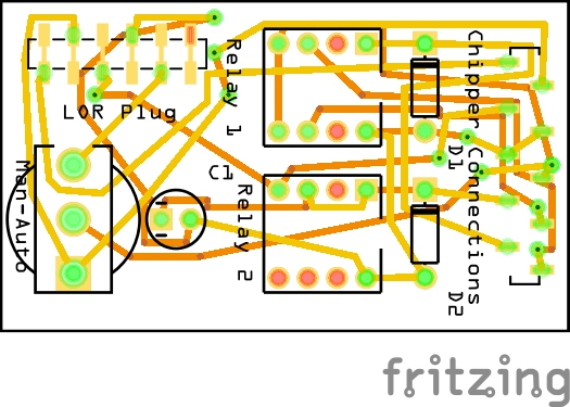
1 Like

Hi Peter,
Sorry I haven’t replied earlier, but was called away on a personal matter.
Wow you have been busy, this is very kind of you, thanks very much.
I’ll have a look at your notes to see how I can improve my skill set, but thanks again for taking the time to do one and explain how you achieved it.
I’ll now go and have a look at it.
Just a quick question, does a design have to work in the breadboard, schematic and PCB sheets? I find that it’s easier to work in the schematic and PCB views, but when you go back to the breadboard view, it looks a mess.
Cheers,
Rich

Hi Barnys1,

Sorry for the delayed reply, I was called away on a personal matter.
Thanks for your suggestion.
Cheers,
Rich

Nope, if you don’t do anything to breadboard it will happily stay a mess (while reflecting changes in the other two views) but not interfere. The danger comes when making changes in more than one view, you are usually best to make all your changes in a single view and once that is done follow the ratsnest lines in the other views (if needed).

Peter

As I have said before “this is not true”. I have never had an issue and always work between views (except never breadboard). It is only if you touch the breadboard view that you have any chance of corrupting the file. If you never touch it you can do anything you want in any other view and NEVER corrupt the file. The warning you should give people is do not work in multiple views if you are using breadboard otherwise have fun and work in any order you like. It is the absolute best part of Fritzing and making people scared of it only makes people not use the software.

If you have experience you can work in any view - even BB - because you can see in your head what happens in other views, but if you are a beginner stick to one view first. We have had to fix some FZ muddled sketches that was more than just user induced error, like a FZ bug. I’ve even made mistakes at the start because sometimes you have a .0100" pined part where you don’t notice the rats is crossed between the pins because it’s so small, and not knowing about the pins being numbered I just connected to any end.

I think it’s when you change a ratsnest to a solid track that FZ gives precedence, i.e. if a part is connected with rats in BB it will change fine in other views, but if it has wires in BB it will try to keep it’s connections in other views.