First attempt at making a full part so dove into Inkscape and the parts editor.
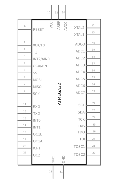
My current avr learning project uses an atmega32 and i couldn’t find one readily so here’s mine. Seems to work for me.
ATmega32.fzpz (14.0 KB)
EDIT: Updated part after changes in this thread available in ATmega32 40 pin DIP part submission
I ran that part through a few quick tests. Starting with FritzingCheckPart, then opening the part and trying to work with it, and manual inspection of the files. Here is a quick summary.
The group and id for the breadboard and schematic views do not exist in the svg files.
Fritzing does not handle font size properly when the text uses a size that includes units. It wants things like style="font-size:27.77;", not "font-size:27.77px;" (or font-size="27.77" not font-size="27.77px"). Applies to both breadboard and schematic svgs here.
The breadboard svg includes a connector0 pin and terminal, but that does not exist in the part definition. The connector0terminal rectangle is set with zero width and height, so it probably can not be selected graphically in Inkscape. By convention the connectors are defined starting from 0, and the pin numbers are one greater.
Fritzing converts, but the latest convention is to use black stroke for pcb silkscreen, not white.
The silkscreen block (layer) should be before (earlier in the file) than the copper layers.
The breadboard svg looks good, and seems functional.
The schematic svg looks ok, but could be done as a more logical view, instead of directly matching the chip pinout. There only needs to be a single gnd (typically on the bottom), the VCC connection at the top. The 2 GND pins should be put into a bus in the definition. The pins for the ports are already (mostly) in a blocks, but they could be moved so that the A,B,C,D ports are all together, with the reset of the pins moved above or below the ports. Maybe port B and D on the left, with port C and D on the right. Add blank space on the left or right (if needed) so that PA0 is directly across from PB0, and PC7 is directly across from PD7. This is a logical view, not physical.
The PCB view looks strange. I see a large red rectangle in the middle of the chip outline. Creating a connection to the pins in other views reflects correctly here, but attempting to create a trace to a pin directly on the pcb view, on the top layer, jumps to the center of that red rectangle. The view functionality is broken.
I expect that the top layer problem is because of the way the copper1 and copper0 layers were created in the pcb svg. Typically, THT parts with identical top and bottom layer pads, have all of the connector (circle) elements created once with their ids, then the whole set is wrapped in a group with the copper0 layer id, then THAT group is wrapped in another group with the copper1 layer id. That puts the connectors on both layers. This svg has separate copper0 and copper1 groups with (apparently) identical content, but the connector ids are only in the copper0 group (or bottom layer). To fix this should be as simple as deleting the existing copper1 group with all of its content, then adding the copper1 group around the copper0 group.
I’ll go back over it and see about straightening things out.
Copper0 group/elements now in Copper1 group. Connector order (everywhere) now back to zero (0) starting point.
A couple of oddities. I can manually move the silkscreen group before the copper1 group but Inkscape keeps wanting to move it after. Why?
In pcb, I’ve got a rectangle for connector0pin but i can’t seem to put it into the copper0 group. I can drag it in, save, close app, open app and pcb file back up and the xml has the pin1 connector0 element back out last in the tree, AND the silkscreen has gotten moved to the end again.
I can use Inkscape, but do not know it at the level this seems to be hitting. I know xml and svg, so for moving things around, I use an xml aware text editor, instead of Inkscape. The only way that I know of that should fix that, would be to completely ungroup the connector elements, make sure that the rectangle element is where you want it, then select the elements and create a group from them. Twice to get both copper0 and copper1.
I have never before seen/heard of a case where Inkscape is changing order of graphics like that.
Thanks. I’ll try that.
I think the pcb is ok now. Working on the schematic. Not 100% sure about it. Looked for some examples of what you were mentioning. Visually/logically is this something along the lines you are talking about for the schematic? Pin #s/no pin #s? (attached)
Yes, that is the general idea for what I was talking about. Pin numbers are optional, and somewhat personal preference. Hovering over a pin will show the associated connector number, name and description. I usually use that, because I have run into parts with pins that are miss-labeled in one or more views. The pin descriptions can be wrong too, but at least I can tell what is the same pin in different views. Pin number labels do get a bit strange for bused connectors (see below). For that, a single schematic pin really connects to multiple physical pins, so choice for label is not obvious.
This example is a work in progress to develop an Arduino UNO (and other) board that is shield friendly. That is, a shield part placed on top of it will properly connect the matching pins, and show those connection on schematic and pcb views.
uno_test.fzpz (27.3 KB)
A few things in the current version of that are of interest here. First, there are 5 pins in the breadboard view that are GND. Click and hold on any one of them highlights all of the others, and wires connected to one are effectively connected to all (also highlighted). That is done using a bus in the part definition file. See Internal connections in the part definition file format.
Next, the part is a ‘board’, but the schematic is almost the same as the bare chip. Except for the ICSP2 header. This shows only a single GND pin. Since the connectors are all on the same internal bus, Fritzing understands that they are connected together, so in the logical / functional schematic view, only a single GND is needed.
There are a couple of ways to implement that. One (commonly used) is to create all 5 pins in the schematic view as normal, but place (stack) them all at the same place. It LOOKS like one pin. The bottom pins can be graphically invisible or not. Only the top one is actually seen. A better (I think) way, is to make the extra copies of the pin invisible in the svg, and mark them as hybrid. See Hybrid connectors in the part definition file format. Only one connector on a bus needs to be ‘normal’ (in schematic view). PCB view as different constraints. There you want (if possible) to have every connector that does not have a pin representation on pcb to be hybrid.
That is less used (or understood). I added to the referenced documentation recently after research and experimentation to find what what the requirements were to make it work. Most of the examples I found were broken one way or another.
Next, the pins on the schematic view are grouped into blocks, similar to what you have already done. An extension to that, especially if you want to use functional names as pin labels, is to add a group label (and maybe bracketing line), to show that the set is all part of eg port B.
Gotcha! I’ll “combine” the GND lines in bus format. Before i made that screenshot i actually had 4 “brackets” with PORTA,… labels but removed them thinking it was getting too much but I’ll put them back and then zip it all up and repost for beta2 review  .
.
Uhg. Something is broke after rearranging the schematic view. When i import the part and drag it into the breadboard it’s blue highlighted. Hover over it it turns red. Schematic view has all the pins red. PCB view when i hover over various pins most of them pop up identity info for PA0. The XML shows silkscreen group, then copper 1 with copper 0 and it’s elements inside.
Is it JUST pin definitions that links one view to the other or are there other critical dependencies from bb to pcb to schematic (document size, etc)?
I gotta look at a couple other part files and see if i spot something.
The svgId values for each view and connector in the part definition link to the elements with matching id values in each view svg. That should be the entire direct linkage. Indirect uses the part definition bus sets, but that is just references the connector ids that are already in the part definition.
It sounds like there might be duplicate connector pin ids. You probably did some copy and paste. Did you miss renaming the copied ids?
Have you got python on your system? You could try running FritzingCheckPart against the files from the part. To see if it spots something.
I do have python. I think I’ve corrected things, least wise when i import the part things match up now no weird stuff happening.ATmega32.fzpz (13.5 KB)
Ignore that one, the port fonts were wrong. Fixed here:
ATmega32.fzpz (13.3 KB)
FritzingCheckPart says the silkscreen is still not black.
There are 4 font-size with ‘px’ units left in the schematic svg. Probably those 4 port name strings you just fixed the font on.
The breadboard and schematic svg files do not have the layer name ids defined, which breaks svg exports.
On pcb view, connector0pin as no radius, so no hole will be exported to gerber
Further inspection finds
The bus definition for the common ground connectors is not in the part definition.
The pins (ports and other side connectors) are not aligned to the standard 0.1 inch spacing. All of the connector terminal elements (and the associated end of the connector pin elements) should be multiples of 0.1 inch apart in both x and y directions.
Quick testing says that the part is generally working, with those issues.
As a side note, you should be able to edit a post or comment here after sending it to the forum. At least for a while (there is a timer that locks them). So you can fix problems like you discovered without a new comment. Just also add a note to show the comment was edited, to warn people they might have gotten the older version.
Having issues getting FritzingCheckpart to run. Seems to hang on line 24 with command not found.
$FritzingCheckpart.py part…fzp
Advice on resolving this please.
To recap:
I believe the silkscreen is ok now.
Removed px units from schematic.
Created “breadboard” and “schematic” groups in those two files containing the layouts.
Fixed pcb connector0
Got the bus defined in the part file with the two ground connectors in it. If i wire parts to each ground the schematic and pcb show the common connection.
Connector spacing: I know what you mean here but I’ve gone through each pin in the pcb and the breadboard and they are multiples of 0.1". I used the ruler and midpoint snapping to verify it was 0.1" from the middle of one pin to the other.
I’ll upload once the check script is running and reports it’s ok.
Do you get anything more than “command not found”? You mention line 24. If not more in the message, what is line 24 in the FritzingCheckPart.py file? (I assume that the FritzingCheckpart.py is a typo, “P” not “p”, that you are running on linux, and that the “$” prefix is actually from the command line prompt).
The breadboard and pcb pins need to be laid out the same as the actual part. Whether that is 0.1 inch spacing or not. The schematic view though, should always use 0.1 inch spacing, so that connection lines to other parts line up consistently. The schematic is where the fix is needed. I managed to leave that detail out of the previous post.
Debug = 0
Ok. I’ll work on the schematic for the spacing.
Thx
Hmm, that is a simple value assignment to a variable., but it is also the first non-comment line in the file. I wonder if the system is trying to execute the python code as a shell script?
Try using python <path/to>/FritzingCheckpart.py part…fzp
or python3 instead of just python, depending how your environment is configured.
Ok that’s working. It corrected several² things and threw a couple warnings. I’ve corrected those, moved the .bak files out of the way and rerun. No errors or warnings. Part imports fine and breadboard connections seem to reflect ok in the schematic and pcb.
Lemme know please if there’s any other item(s) i needs to address. Here’s the updated zip file
ATmega32.fzpz (13.9 KB)
A quick test and inspection says that is all working fine.
My process for running FritzingCheckPart, is to move to a working directory, delete everything left hanging around from the previous time, unzip the fzpz, then run FritzingCheckPart against the fzp.
Some things to note for later, or that might act a bit different than you expect.
You have specified at label of “Atmega32” in the part definition. However, that label is really the prefix that Fritzing using to differentiate between multiple copies of the part in a single sketch. It also trims any digits from the end before it uses the label, so what gets into the sketch is actually “Atmega1” then “Atmega2”. Since this is a bare chip, a label of just “U” is common. Since this is a microcontroller, you could go fancier with a label of “uC”, or (Fritzing handles utf characters) “µC”. The part labels used in the Fritzing views can be configured individually (by view and by instance of a part) to include anything from the properties, so including “chip label” may be what you want, instead of setting the full part “label” to Atmega32.
If you want to have the chip label automatically (initially) shown with the part label (along with the part label plus sequential number), you can add ‘showInLabel=“yes”’ to the attributes for the property. See Part Properties documentation.
You set the bus id to “bus0”. That can be any text, so you could have set the id to “GND” or “Ground”, to provide context on what the bus contains.
You have a tag in the definition for “through-hole”. You might want to replace that with (or add) “tht”.