
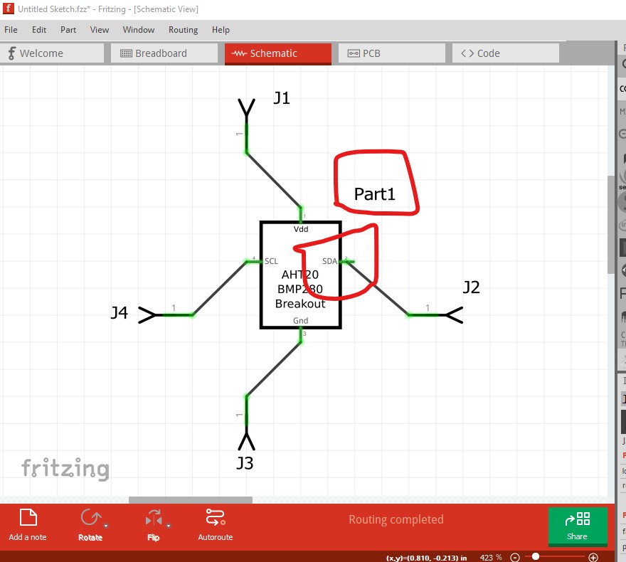
A few problems. Schematic is missing a terminalId on SDA which causes the wire to connect in the center of the pin rather than the end. The fzp file needs a label field with “A” (for assembly) in it to replace part1
pcb is incorrectly scaled and the holes are too small.
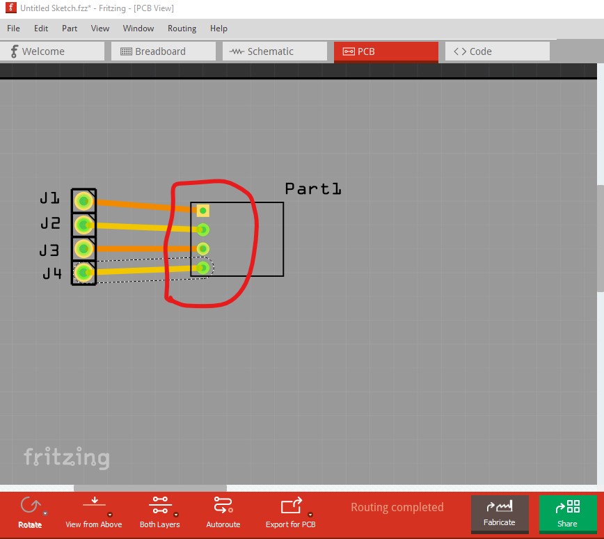
The pins should line up with the headers and the hole size should be 0.038in not the current 0.026in. Instructions on correcting this can be found here:
Peter
thank you.
here is the update
AHT20-BMP280_breakout.fzpz (9,9 Ko)
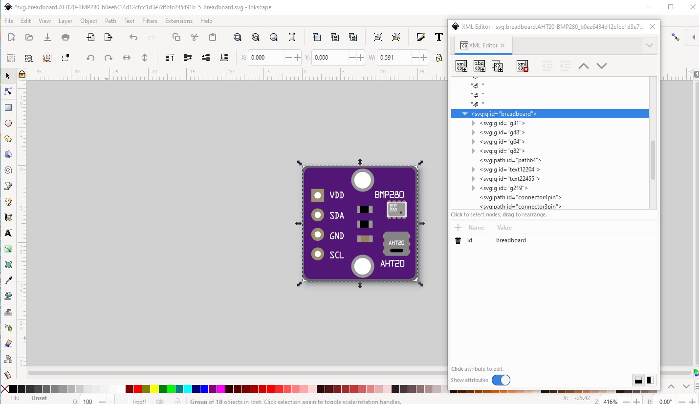
Still a few problems. The pcb svg is dimensioned in px which can cause scaling problems if Fritzing guess wrong on the dpi value (which it looks to be doing here.) The breadboard svg is missing a layerId (which will cause the part to not export as an image. FritzingCheckPart.py notes both of these:
Warning 19: File
‘svg.pcb.AHT20-BMP280_b0ee6434d12cfcc1d3e7dfbfc245491b_5_pcb.svg.bak’
At line 3
Height 56.692913 is defined in px
in or mm is a better option (px can cause scaling problems!)
Warning 19: File
‘svg.pcb.AHT20-BMP280_b0ee6434d12cfcc1d3e7dfbfc245491b_5_pcb.svg.bak’
At line 3
Width 56.692913 is defined in px
in or mm is a better option (px can cause scaling problems!)
Error 69: File
‘svg.breadboard.AHT20-BMP280_b0ee6434d12cfcc1d3e7dfbfc245491b_5_breadboard.svg.bak’
At line 29
Found a drawing element before a layerId (or no layerId)
Error 18: File
‘part.AHT20-BMP280_9cd80e753c95b7f0490b99b444cb6f16_13.fzp.bak’
Connector connector2terminal is in the fzp file but not the svg file. (typo?)
svg svg.pcb.AHT20-BMP280_b0ee6434d12cfcc1d3e7dfbfc245491b_5_pcb.svg.bak
as well as a not needed terminalId in pcb (which will be ignored but is incorrect.) As well the hole size in pcb is now too large at 0.048889in. Assuming you are using Inkscape the holesize is set as
hole_size = pad-diameter - (2 * stroke-width)
Breadboard needs a layerId from this:

to this (Edit->select all, Object->group and set the group id to breadboard)
pcb needs this to change from px to in from this
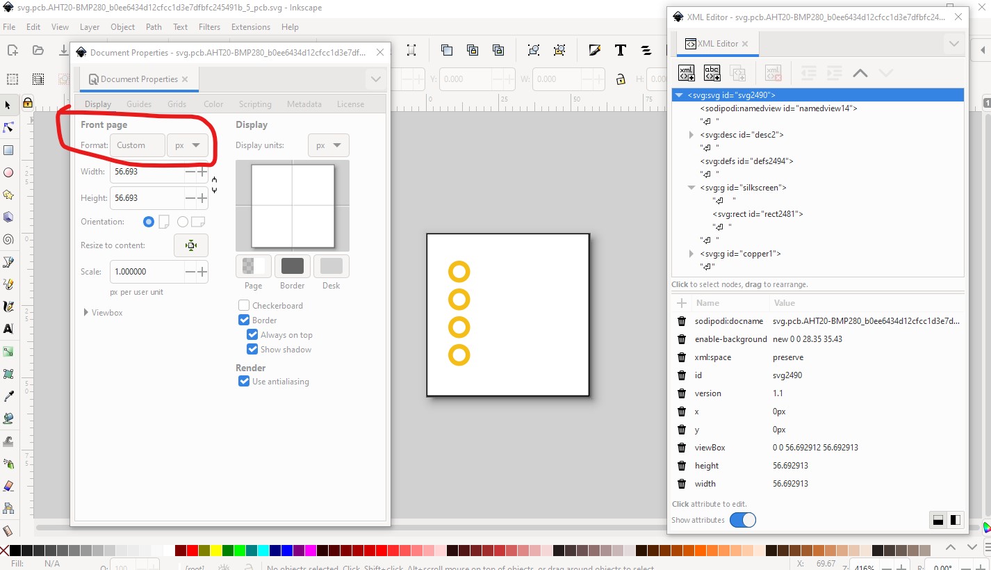
to this
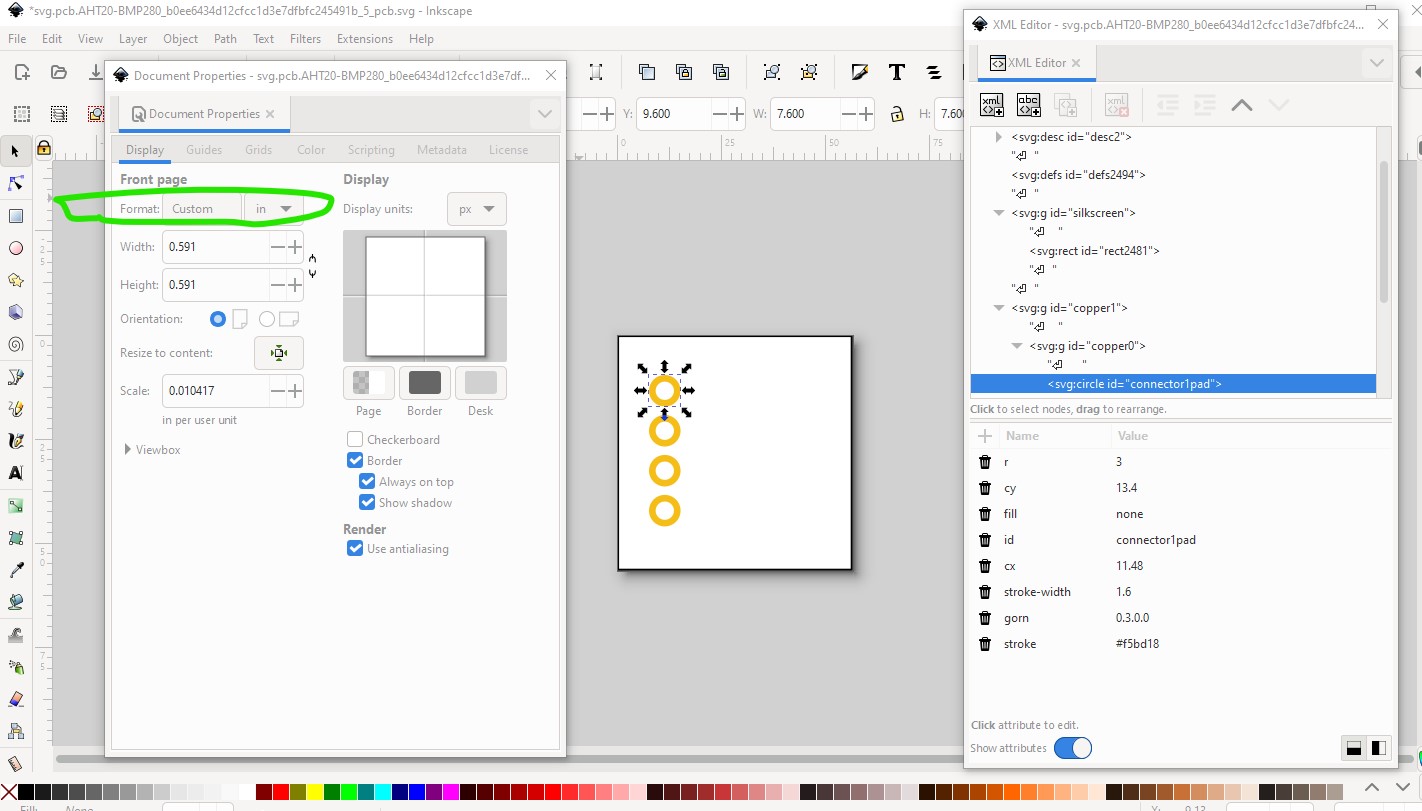
and then have the pads moved to be on 0.1in boundaries. Pads should have a stoke-width of 20 thousands of an inch and a hole size of 0.038in and be on a 0.1in boundary between pads. As well the rectangle in silkscreen needs a stroke of #000000 (black) and a stroke width of 10 thousandths.
Peter
Hi Vanepp,
thank you for your useful tool FritzingCheckPart.py
i did the change
just one line :
“This is a through hole part as both copper0 and copper1 views are present.
If you wanted a smd part remove the copper0 definition from line 43”
how can i modify that ?
AHT20-BMP280_breakout.fzpz (8,8 Ko)
The new version looks clean.
No need to do anything, this is a through hole part. I will probably remove that message (or at least change it) as it currently only causes confusion. The intent is to tell you whether Fritzing thinks the part is through hole (both copper1 and copper0 present) or SMD (only copper1 present.) It is possible (and a mistake!) to have both copper1 and copper0 defined in the pcb layer property but only use copper1 in the connector definitions. This is intended to tell you which Fritzing thinks your part is, but as noted mostly causes confusion and needs to be changed somehow.
Peter