Does anyone have Fritzing parts for these 7-segment LED displays:
4-digit: HS420561K
3-digit: HS420561K
2-digit: HX220561K
Does anyone have Fritzing parts for these 7-segment LED displays:
4-digit: HS420561K
3-digit: HS420561K
2-digit: HX220561K
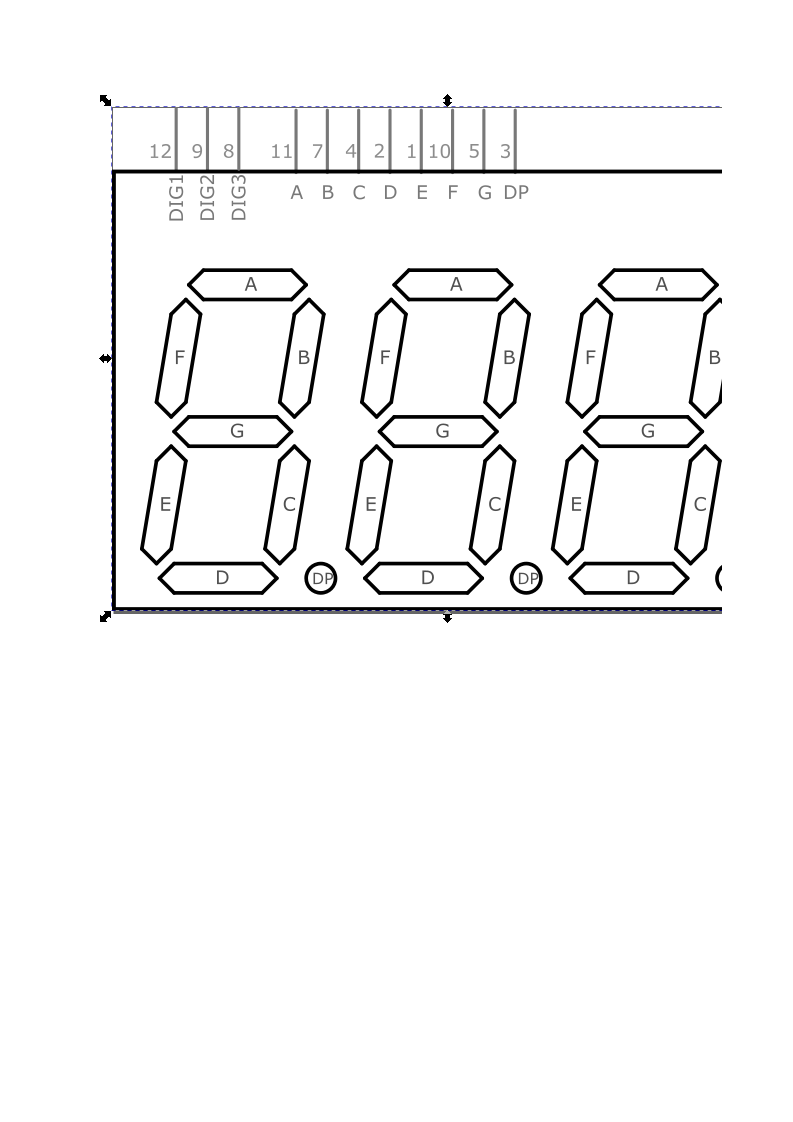
I had a go at making a 3-digit 7-segment part, using Inkscape. I created the images which looked OK in Inkscape, the PCB image is fine:
We can not tell what is wrong with the svg when what you posted was a png. If the forum will not accept the svg directly, rename to append .zip to the name. An initial guess is a problem with the units for the image file, or the font used for the text.
Sorry, here’s the SVG file.
![]()
I ran the svg through a part checker script we have. It reports several errors. Here is a summary, with the duplicates removed.
f4e06a10b1b8ada6c8bff20a7b899c4f3bed20a3.svg'
At line 57
Removed px from font-size leaving 60
The font-size attribute should contain just a number, without any units. There are 46 cases of this, mostly with size 60, but a few with 50 or 59.«something». Just need to remove the “px” after the size values, though might was to change those 59.x values to 60.
f4e06a10b1b8ada6c8bff20a7b899c4f3bed20a3.svg'
At line 119
Key -inkscape-font-specification
value 'Droid Sans, Normal' is invalid
Inkscape got too smart, and added an inkscape specific font specification that is not compatible with Fritzing. 11 cases. Just need to remove the “-inkscape-font-specification:‘Droid Sans, Normal’;” entries.
f4e06a10b1b8ada6c8bff20a7b899c4f3bed20a3.svg'
At line 123

Apparant nested tspan which fritzing doesn't support
If your text doesn't appear in Fritzing this is probably why
Fritzing does not support tspan elements. 11 cases. Text content needs to be directly in a text element. Replace the whole tspan element with just the text that it contains. This could cause the text to move (if the tspan coordinates are not the same as text element), so need to check and adjust that afterwards.
f4e06a10b1b8ada6c8bff20a7b899c4f3bed20a3.svg'
At line 12

Found a drawing element before a layerId (or no layerId)
You wrapped the content in a group, but did not add the “schematic” id to the group.
The checker tools automatically fixed the first 2 cases. I manually cleaned up the last 2. Here is the result. Give it a try, to see if the issues go away.
![]()
Thank you @microMerlin that was a real help, much appreciated. Are you able to share the part checker script, or is it freely available (I haven’t checked yet)?
Also, thank you to @Old_Grey watched the video and that too was very helpful.
I’ve not created parts before, and it is quite satisfying.
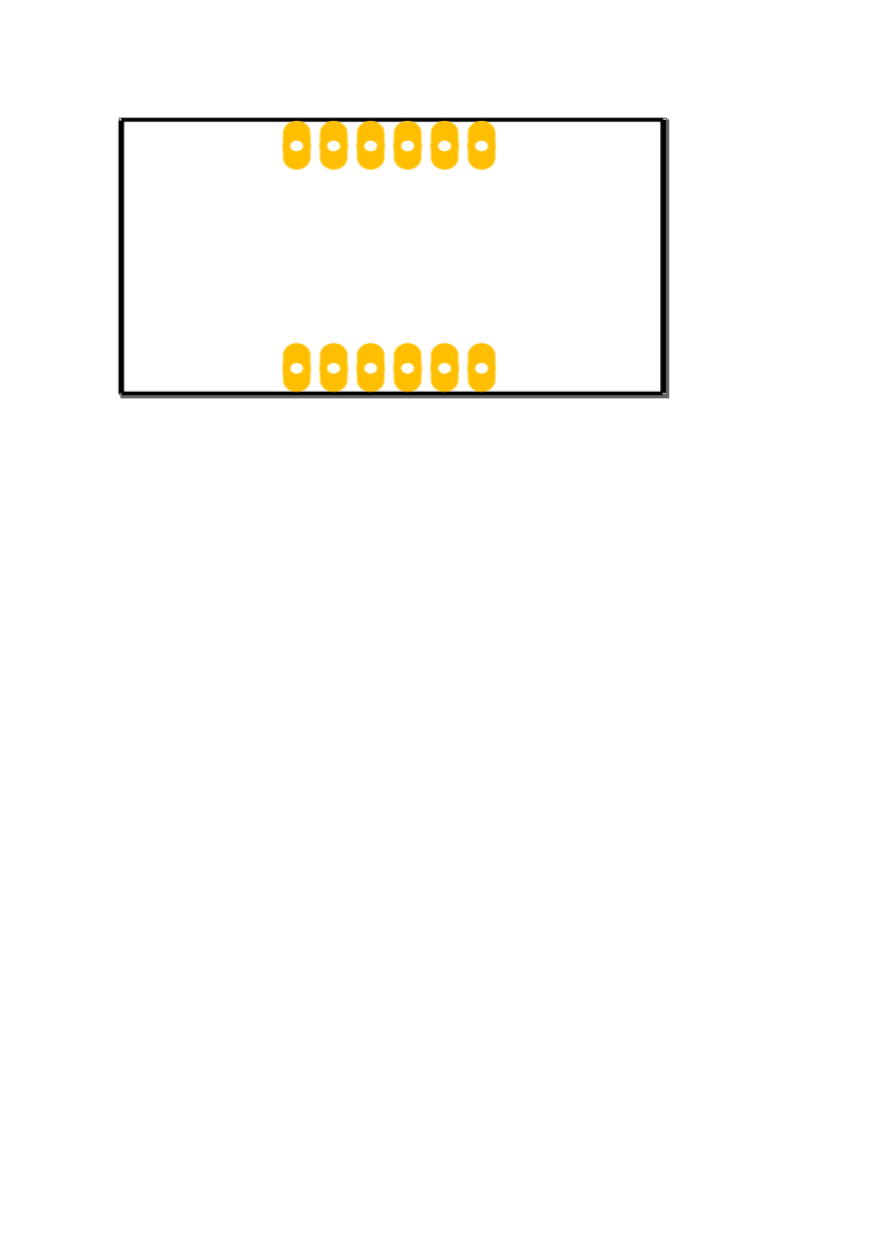
I have been finishing off both the 3-digit 7-segment LED as well as a 4-digit version. All appeared to be going well until I sent a PCB image to PDF and then the pads appear odd, although they look OK both in Inkscape and Fritzing! This is what the PDF image looks like:
I have attached the part.
FritzingCheckPart is a python script available in its own github repository.
What you attached to the previous command was only the xml part definition file, not the full part. The full part would be an fzpz file, which is a zip with the fzp plus the view svg files inside.
From the symptoms in that screenshot, I am guessing you hit one of the Fritzing bugs, where it does not handle some specific conditions in valid svg path elements. I did some work on that for Design Rules Check. This looks like it might be similar, but need the full part file to be able to check. I am not currently setup to do debug/trace on pdf export, but may be able to narrow down by manual adjustment to the problem path elements. As a check, to see some of the scope of the problem, what does it look like when exported to jpeg or svg? Or to gerber. Some of the code is common, some is different for those options.
@microMerlin sorry for attaching the wrong file. The attached should be the full part, both 3-digit & 4-digit, I created earlier. When generating Gerber files and viewing in an a Gerber viewer I see the same issue with the pads.
HS320561K.fzpz (16.6 KB) HS420561K.fzpz (17.8 KB)
You can’t use ellipse for pads in FZ - FZ won’t understand them -, so they have to be changed to circle.
Groups and group labels aren’t right, especially in the 3 digit. You might have to ungroup and regroup things, but all things that aren’t contact pins go into a group called silkscreen. And all contacts go into a group called copper0, which has to be grouped again and called copper1.
You can use the free Gerbv viewer to check if parts are going to be rendered correctly.
I ran the HS320561K part through FritzingCheckPart. That got a lot of complaints. Looking at the svg files, I found there were multiple layers of group in group in group … wrapped around whole file content, and blocks of graphics within files.
“copper1” groups exist in breadboard and icon images, as well as pcb. The pcb image has a copper0 group inside of copper1, implying through hole, but the copper0 group is empty. The copper elements all exist on only the one side (bottom) of the board. The fzp file information indicates that the connectors should be on both sides.
Loading the part into Frtizing, and examining the results, pin 6 connector is missing in all views. In pcb view, the expanded ellipse pad exists, but not the connector. I see a “connector0pad-4-4” ellipse, which is probably supposed to be that missing connector5 = pin6. If that is a “no connect” pin, it should exist, and be tagged as such, in at least breadboard and pcb views. The schematic view of the part is rather over sized. It should be more of symbolic view, instead of those drawn shapes for each segment. In breadboard view, the connector pins are bigger than they should be. I schematic view, the pins (lines) are not aligned to the standard 0.1 in spacing.
The fzp title element should be a description of the part, not the part number. The label should be prefix used to tag instances of the part (along with a sequential number). Something like “disp”, so multiple instances would become disp1, disp2, … Duplicating the part number in the variant is not needed. For this, variant does not need to exist. It would be used to identify variations that would otherwise have identical attributes.
The definition information says 300mil spacing. Breadboard looks like 400mil spacing (possibly from those px units). pcb view looks like 600mil spacing.
With both your original, and my modified version, exporting the pcb view looks good for jpg, png, pdf, but I see your glitch on the svg export. Examining the source and created path elements, I do not see anything specific that Fritzing should choke on, but the different structure says it dropped some segments of the path. Which would be a bug.
I used inkscape to ungroup those groups multiple times, deleted the empty copper group, then regrouped the pcb elements to get the non-silkscreen elements inside a copper0 group, which is inside of a copper1 group. After that, I ran FritzingCheckPart on the result. The full report after that is below, with the file paths truncated to shorten the lines. Here is a summary of what it says.
% FritzingCheckPart …/part.HS320561K_740433510e6913850aacb34dc1d42eaf_12.fzp
Processing "…/part.HS320561K_740433510e6913850aacb34dc1d42eaf_12.fzp"
File
'…/part.HS320561K_740433510e6913850aacb34dc1d42eaf_12.fzp.bak'

This is a through hole part as both copper0 and copper1 views are present.

If you wanted a smd part remove the copper0 definition from line 49

Warning 7: File
'…/part.HS320561K_740433510e6913850aacb34dc1d42eaf_12.fzp.bak'
At line 2

No Fritzing version in fzp file

Warning 19: File
'…/svg.breadboard.HS320561K_c4b652af30a5f0e3ceaa988c37267ec3_2_breadboard.svg.bak'
At line 17

Height 47.262985 is defined in px

in or mm is a better option (px can cause scaling problems!)

Warning 19: File
'…/svg.breadboard.HS320561K_c4b652af30a5f0e3ceaa988c37267ec3_2_breadboard.svg.bak'
At line 17

Width 107.63095 is defined in px

in or mm is a better option (px can cause scaling problems!)

Error 64: File
'…/part.HS320561K_740433510e6913850aacb34dc1d42eaf_12.fzp.bak'
Connector5 doesn't exist when it must to stay in sequence

Error 69: File
'…/svg.breadboard.HS320561K_c4b652af30a5f0e3ceaa988c37267ec3_2_breadboard.svg.bak'
At line 78

Found a drawing element before a layerId (or no layerId)

Error 18: File
'…/part.HS320561K_740433510e6913850aacb34dc1d42eaf_12.fzp.bak'
Connector connector0terminal is in the fzp file but not the svg file. (typo?)

svg …/svg.breadboard.HS320561K_c4b652af30a5f0e3ceaa988c37267ec3_2_breadboard.svg.bak
Error 18: File
'…/part.HS320561K_740433510e6913850aacb34dc1d42eaf_12.fzp.bak'

Connector connector1terminal is in the fzp file but not the svg file. (typo?)

svg …/svg.breadboard.HS320561K_c4b652af30a5f0e3ceaa988c37267ec3_2_breadboard.svg.bak
Error 18: File
'…/part.HS320561K_740433510e6913850aacb34dc1d42eaf_12.fzp.bak'

Connector connector2terminal is in the fzp file but not the svg file. (typo?)

svg …/svg.breadboard.HS320561K_c4b652af30a5f0e3ceaa988c37267ec3_2_breadboard.svg.bak
Error 18: File
'…/part.HS320561K_740433510e6913850aacb34dc1d42eaf_12.fzp.bak'

Connector connector3terminal is in the fzp file but not the svg file. (typo?)

svg …/svg.breadboard.HS320561K_c4b652af30a5f0e3ceaa988c37267ec3_2_breadboard.svg.bak
Error 18: File
'…/part.HS320561K_740433510e6913850aacb34dc1d42eaf_12.fzp.bak'

Connector connector4terminal is in the fzp file but not the svg file. (typo?)

svg …/svg.breadboard.HS320561K_c4b652af30a5f0e3ceaa988c37267ec3_2_breadboard.svg.bak
Error 18: File
'…/part.HS320561K_740433510e6913850aacb34dc1d42eaf_12.fzp.bak'

Connector connector6terminal is in the fzp file but not the svg file. (typo?)

svg …/svg.breadboard.HS320561K_c4b652af30a5f0e3ceaa988c37267ec3_2_breadboard.svg.bak
Error 18: File
'…/part.HS320561K_740433510e6913850aacb34dc1d42eaf_12.fzp.bak'

Connector connector7terminal is in the fzp file but not the svg file. (typo?)

svg …/svg.breadboard.HS320561K_c4b652af30a5f0e3ceaa988c37267ec3_2_breadboard.svg.bak
Error 65: File
'…/svg.pcb.HS320561K_c4b652af30a5f0e3ceaa988c37267ec3_2_pcb.svg.bak'
At line 133

Connector connector6pin is an ellipse not a circle, (gerber generation will break.)

Error 74: File
'…/svg.pcb.HS320561K_c4b652af30a5f0e3ceaa988c37267ec3_2_pcb.svg.bak'
At line 133

Connector connector6pin has no radius no hole will be generated

Error 65: File
'…/svg.pcb.HS320561K_c4b652af30a5f0e3ceaa988c37267ec3_2_pcb.svg.bak'
At line 154

Connector connector9pin is an ellipse not a circle, (gerber generation will break.)

Error 74: File
'…/svg.pcb.HS320561K_c4b652af30a5f0e3ceaa988c37267ec3_2_pcb.svg.bak'
At line 154

Connector connector9pin has no radius no hole will be generated

Error 65: File
'…/svg.pcb.HS320561K_c4b652af30a5f0e3ceaa988c37267ec3_2_pcb.svg.bak'
At line 175

Connector connector11pin is an ellipse not a circle, (gerber generation will break.)

Error 74: File
'…/svg.pcb.HS320561K_c4b652af30a5f0e3ceaa988c37267ec3_2_pcb.svg.bak'
At line 175

Connector connector11pin has no radius no hole will be generated

Error 65: File
'…/svg.pcb.HS320561K_c4b652af30a5f0e3ceaa988c37267ec3_2_pcb.svg.bak'
At line 196

Connector connector7pin is an ellipse not a circle, (gerber generation will break.)

Error 74: File
'…/svg.pcb.HS320561K_c4b652af30a5f0e3ceaa988c37267ec3_2_pcb.svg.bak'
At line 196

Connector connector7pin has no radius no hole will be generated

Error 65: File
'…/svg.pcb.HS320561K_c4b652af30a5f0e3ceaa988c37267ec3_2_pcb.svg.bak'
At line 217

Connector connector10pin is an ellipse not a circle, (gerber generation will break.)

Error 74: File
'…/svg.pcb.HS320561K_c4b652af30a5f0e3ceaa988c37267ec3_2_pcb.svg.bak'
At line 217

Connector connector10pin has no radius no hole will be generated

Error 65: File
'…/svg.pcb.HS320561K_c4b652af30a5f0e3ceaa988c37267ec3_2_pcb.svg.bak'
At line 238

Connector connector0pin is an ellipse not a circle, (gerber generation will break.)

Error 74: File
'…/svg.pcb.HS320561K_c4b652af30a5f0e3ceaa988c37267ec3_2_pcb.svg.bak'
At line 238

Connector connector0pin has no radius no hole will be generated

Error 65: File
'…/svg.pcb.HS320561K_c4b652af30a5f0e3ceaa988c37267ec3_2_pcb.svg.bak'
At line 280

Connector connector3pin is an ellipse not a circle, (gerber generation will break.)

Error 74: File
'…/svg.pcb.HS320561K_c4b652af30a5f0e3ceaa988c37267ec3_2_pcb.svg.bak'
At line 280

Connector connector3pin has no radius no hole will be generated

Error 65: File
'…/svg.pcb.HS320561K_c4b652af30a5f0e3ceaa988c37267ec3_2_pcb.svg.bak'
At line 301

Connector connector1pin is an ellipse not a circle, (gerber generation will break.)

Error 74: File
'…/svg.pcb.HS320561K_c4b652af30a5f0e3ceaa988c37267ec3_2_pcb.svg.bak'
At line 301

Connector connector1pin has no radius no hole will be generated

Error 65: File
'…/svg.pcb.HS320561K_c4b652af30a5f0e3ceaa988c37267ec3_2_pcb.svg.bak'
At line 322

Connector connector4pin is an ellipse not a circle, (gerber generation will break.)

Error 74: File
'…/svg.pcb.HS320561K_c4b652af30a5f0e3ceaa988c37267ec3_2_pcb.svg.bak'
At line 322

Connector connector4pin has no radius no hole will be generated

Error 65: File
'…/svg.pcb.HS320561K_c4b652af30a5f0e3ceaa988c37267ec3_2_pcb.svg.bak'
At line 343

Connector connector2pin is an ellipse not a circle, (gerber generation will break.)

Error 74: File
'…/svg.pcb.HS320561K_c4b652af30a5f0e3ceaa988c37267ec3_2_pcb.svg.bak'
At line 343

Connector connector2pin has no radius no hole will be generated

Error 65: File
'…/svg.pcb.HS320561K_c4b652af30a5f0e3ceaa988c37267ec3_2_pcb.svg.bak'
At line 364

Connector connector12pin is an ellipse not a circle, (gerber generation will break.)

Error 74: File
'…/svg.pcb.HS320561K_c4b652af30a5f0e3ceaa988c37267ec3_2_pcb.svg.bak'
At line 364

Connector connector12pin has no radius no hole will be generated
Here is the part with the described adjustments. It is not correct yet. It only has the nested group and pcb copper 0 stuff cleaned up.
HS320561K-2.fzpz (18.1 KB)
I said the glitch is a bug. However similar structures work elsewhere, even the second row of pins in this part. So it should be possible to build those paths differently to avoid whatever is triggering the glitch.
Thank you @microMerlin for all your help.
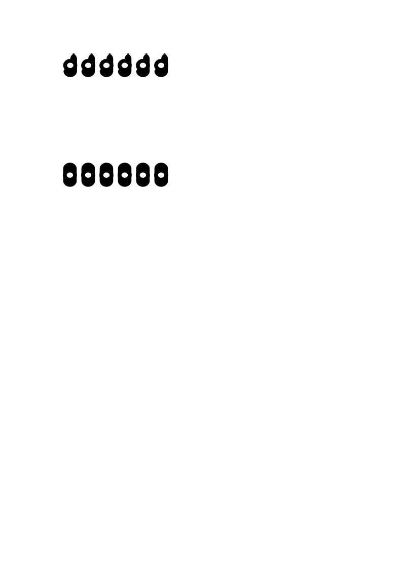
I roughly did one pad in PCB to show you how the pad fault corrects if drawn correctly.
HS320561K-3.fzpz (15.9 KB)
Thanks @Old_Grey that was pin7 you drew correctly, right?
I’m starting from scratch and starting on the schematic view. Using a 0.1 inch grid to ensure it’s correct, with a line stroke of 0.25 mm. I’m also going to use meaningful ids for each part in the xml structure to keep track and what is what. Going to do this carefully from now on.
What I had created before was a good learning ground.
I have this afternoon created this 2-digit 7-segment LED part. Thanks to @Old_Grey the pads now show in the PDF images as good. Thanks to @microMerlin for your help as well. I haven’t run the parts checker over this, as I haven’t got the environment setup to run that yet.
I will create the 3-digit and 4-digit variants of the 7-segment LED another day.
7-Segment-Display-2-Red.fzpz (11.0 KB)
Below is the report from FritzingCheckPart on your new version. Summary and translation (where different from previous):
% FritzingCheckPart.sh …/part.HS220561K_9b599e9d04c0f9a3f069a44cb1139b70_5.fzp
File
'…/part.HS220561K_9b599e9d04c0f9a3f069a44cb1139b70_5.fzp.bak'

This is a through hole part as both copper0 and copper1 views are present.

If you wanted a smd part remove the copper0 definition from line 46

Warning 7: File
'…/part.HS220561K_9b599e9d04c0f9a3f069a44cb1139b70_5.fzp.bak'
At line 2

No Fritzing version in fzp file

Warning 20: File
'…/svg.pcb.HS220561K_9b599e9d04c0f9a3f069a44cb1139b70_10_pcb.svg.bak'
At line 22

copper1 layer should be at the top, not under group silkscreen

Error 64: File
'…/part.HS220561K_9b599e9d04c0f9a3f069a44cb1139b70_5.fzp.bak'

Connector8 doesn't exist when it must to stay in sequence

Error 18: File
'…/part.HS220561K_9b599e9d04c0f9a3f069a44cb1139b70_5.fzp.bak'

Connector connector0terminal is in the fzp file but not the svg file. (typo?)

svg …/svg.breadboard.HS220561K_9b599e9d04c0f9a3f069a44cb1139b70_10_breadboard.svg.bak

Error 18: File
'…/part.HS220561K_9b599e9d04c0f9a3f069a44cb1139b70_5.fzp.bak'

Connector connector1terminal is in the fzp file but not the svg file. (typo?)

svg …/svg.breadboard.HS220561K_9b599e9d04c0f9a3f069a44cb1139b70_10_breadboard.svg.bak

Error 18: File
'…/part.HS220561K_9b599e9d04c0f9a3f069a44cb1139b70_5.fzp.bak'

Connector connector2terminal is in the fzp file but not the svg file. (typo?)

svg …/svg.breadboard.HS220561K_9b599e9d04c0f9a3f069a44cb1139b70_10_breadboard.svg.bak

Error 18: File
'…/part.HS220561K_9b599e9d04c0f9a3f069a44cb1139b70_5.fzp.bak'

Connector connector3terminal is in the fzp file but not the svg file. (typo?)

svg …/svg.breadboard.HS220561K_9b599e9d04c0f9a3f069a44cb1139b70_10_breadboard.svg.bak

Error 18: File
'…/part.HS220561K_9b599e9d04c0f9a3f069a44cb1139b70_5.fzp.bak'

Connector connector4terminal is in the fzp file but not the svg file. (typo?)

svg …/svg.breadboard.HS220561K_9b599e9d04c0f9a3f069a44cb1139b70_10_breadboard.svg.bak

Error 18: File
'…/part.HS220561K_9b599e9d04c0f9a3f069a44cb1139b70_5.fzp.bak'

Connector connector5terminal is in the fzp file but not the svg file. (typo?)

svg …/svg.breadboard.HS220561K_9b599e9d04c0f9a3f069a44cb1139b70_10_breadboard.svg.bak

Error 18: File
'…/part.HS220561K_9b599e9d04c0f9a3f069a44cb1139b70_5.fzp.bak'

Connector connector6terminal is in the fzp file but not the svg file. (typo?)

svg …/svg.breadboard.HS220561K_9b599e9d04c0f9a3f069a44cb1139b70_10_breadboard.svg.bak

Error 18: File
'…/part.HS220561K_9b599e9d04c0f9a3f069a44cb1139b70_5.fzp.bak'

Connector connector7terminal is in the fzp file but not the svg file. (typo?)

svg …/svg.breadboard.HS220561K_9b599e9d04c0f9a3f069a44cb1139b70_10_breadboard.svg.bak

Error 69: File
'…/svg.schematic.HS220561K_9b599e9d04c0f9a3f069a44cb1139b70_10_schematic.svg.bak'
At line 7

Found a drawing element before a layerId (or no layerId)

Error 74: File
'…/svg.pcb.HS220561K_9b599e9d04c0f9a3f069a44cb1139b70_10_pcb.svg.bak'
At line 24

Connector connector10pin has no radius no hole will be generated

Error 74: File
'…/svg.pcb.HS220561K_9b599e9d04c0f9a3f069a44cb1139b70_10_pcb.svg.bak'
At line 26

Connector connector9pin has no radius no hole will be generated

Error 74: File
'…/svg.pcb.HS220561K_9b599e9d04c0f9a3f069a44cb1139b70_10_pcb.svg.bak'
At line 28

Connector connector7pin has no radius no hole will be generated

Error 74: File
'…/svg.pcb.HS220561K_9b599e9d04c0f9a3f069a44cb1139b70_10_pcb.svg.bak'
At line 30

Connector connector6pin has no radius no hole will be generated

Error 74: File
'…/svg.pcb.HS220561K_9b599e9d04c0f9a3f069a44cb1139b70_10_pcb.svg.bak'
At line 32

Connector connector5pin has no radius no hole will be generated

Error 74: File
'…/svg.pcb.HS220561K_9b599e9d04c0f9a3f069a44cb1139b70_10_pcb.svg.bak'
At line 34

Connector connector0pin has no radius no hole will be generated

Error 74: File
'…/svg.pcb.HS220561K_9b599e9d04c0f9a3f069a44cb1139b70_10_pcb.svg.bak'
At line 36

Connector connector1pin has no radius no hole will be generated

Error 74: File
'…/svg.pcb.HS220561K_9b599e9d04c0f9a3f069a44cb1139b70_10_pcb.svg.bak'
At line 38

Connector connector2pin has no radius no hole will be generated

Error 74: File
'…/svg.pcb.HS220561K_9b599e9d04c0f9a3f069a44cb1139b70_10_pcb.svg.bak'
At line 40

Connector connector3pin has no radius no hole will be generated

Error 74: File
'…/svg.pcb.HS220561K_9b599e9d04c0f9a3f069a44cb1139b70_10_pcb.svg.bak'
At line 42

Connector connector4pin has no radius no hole will be generated
Thank you again @microMerlin I will change what’s required tomorrow sometime. I will have to setup the environment to be able to run the parts checker myself, but getting there and learning a new skill on the way.