Thank you @Old_Grey I’ll sort that out later.
I think I’ve managed to get there. I have revised the 2-digit part this evening and on using the FritzingCheckPart utility I only now get the output as below. Hopefully I can now move on to the 3 & 4 digit versions. The two warnings re drawing elements appear to be referring to the metedata
pi@raspberrypi:/ $ FritzingCheckPart.py /tmp/part.HS220561K_9b599e9d04c0f9a3f069a44cb1139b70_5.fzp
File
'/tmp/part.HS220561K_9b599e9d04c0f9a3f069a44cb1139b70_5.fzp.bak'

This is a through hole part as both copper0 and copper1 views are present.
If you wanted a smd part remove the copper0 definition from line 46

Modified 4: File
'/tmp/svg.breadboard.HS220561K_9f0f66f37840958401e8a7822b728749_2_breadboard.svg.bak'
At line 4

ReferenceFile

'HS220561K_breadboard.svg'

doesn't match input file

'svg.breadboard.HS220561K_9f0f66f37840958401e8a7822b728749_2_breadboard.svg'

Corrected

Modified 4: File
'/tmp/svg.schematic.HS220561K_9f0f66f37840958401e8a7822b728749_2_schematic.svg.bak'
At line 4

ReferenceFile

'HS220561K.svg'

doesn't match input file

'svg.schematic.HS220561K_9f0f66f37840958401e8a7822b728749_2_schematic.svg'

Corrected

Modified 4: File
'/tmp/svg.pcb.HS220561K_9f0f66f37840958401e8a7822b728749_2_pcb.svg.bak'
At line 4

ReferenceFile

'HS220561K_pcb.svg'

doesn't match input file

'svg.pcb.HS220561K_9f0f66f37840958401e8a7822b728749_2_pcb.svg'

Corrected

Warning 6: File
'/tmp/part.HS220561K_9b599e9d04c0f9a3f069a44cb1139b70_5.fzp.bak'
At line 2

ReferenceFile name

'generic_ic_dip_8_300mil.fzp'

Doesn't match fzp filename

'HS220561K_9b599e9d04c0f9a3f069a44cb1139b70_5.fzp'

Warning 7: File
'/tmp/part.HS220561K_9b599e9d04c0f9a3f069a44cb1139b70_5.fzp.bak'
At line 2

No Fritzing version in fzp file


Error 69: File
'/tmp/svg.breadboard.HS220561K_9f0f66f37840958401e8a7822b728749_2_breadboard.svg.bak'
At line 21

Found a drawing element before a layerId (or no layerId)

Error 69: File
'/tmp/svg.schematic.HS220561K_9f0f66f37840958401e8a7822b728749_2_schematic.svg.bak'
At line 7

Found a drawing element before a layerId (or no layerId)

pi@raspberrypi:/ $
7-Segment-Display-2-Red.fzpz (11.3 KB)
It is not the metadata triggering the layerId errors.
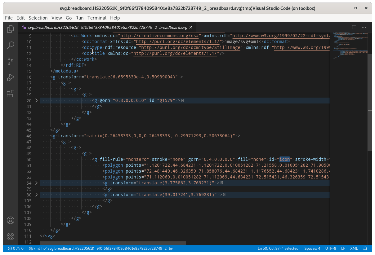
The breadboard svg does not actually contain a “breadboard” id. That also currently has 2 top level group elements, each with multiple nested group elements. One of which has an “icon” id, which does not belong here. There is no place to directly put the id=“breadboard” attribute. It would have to be put on another outer wrapper group. All of the wrapper groups are not needed. In inkscape, you can select a group object, and “ungroup” multiple times. Ungrouping ripples the transform from the group to the ungrouped objects, so nothing moves doing that. After ungrouping a whole lot, you can then do a “select all” and a single “group” to wrap it up. Then added the layer name to that single group as the “id” attribute.
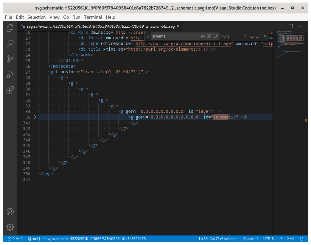
The schematic svg does have a layer id, but it is (again) wrapped inside of multiple outer groups. Something in that is treated as a “drawing element” by the checking tool. Same solution. Ungroup multiple times, then select all and wrap with a single group, with the id=“schematic” attribute.
This time hopefully I’ve managed to produce the 2 digit 7-segment LED Fritzing part.
I don’t get any errors with FritzingCheckPart script:
pi@raspberrypi:/tmp/parts $ FritzingCheckPart.py /tmp/parts/part.HS220561K_9b599e9d04c0f9a3f069a44cb1139b70_5.fzp
File
'/tmp/parts/part.HS220561K_9b599e9d04c0f9a3f069a44cb1139b70_5.fzp.bak'

This is a through hole part as both copper0 and copper1 views are present.
If you wanted a smd part remove the copper0 definition from line 46

Modified 4: File
'/tmp/parts/svg.breadboard.HS220561K_de440744f1e13afc497791de140725a3_3_breadboard.svg.bak'
At line 4

ReferenceFile

'HS220561K_breadboard.svg'

doesn't match input file

'svg.breadboard.HS220561K_de440744f1e13afc497791de140725a3_3_breadboard.svg'

Corrected

Modified 4: File
'/tmp/parts/svg.schematic.HS220561K_de440744f1e13afc497791de140725a3_3_schematic.svg.bak'
At line 4

ReferenceFile

'HS220561K_schematic.svg'

doesn't match input file

'svg.schematic.HS220561K_de440744f1e13afc497791de140725a3_3_schematic.svg'

Corrected

Modified 4: File
'/tmp/parts/svg.pcb.HS220561K_de440744f1e13afc497791de140725a3_3_pcb.svg.bak'
At line 4

ReferenceFile

'HS220561K_pcb.svg'

doesn't match input file

'svg.pcb.HS220561K_de440744f1e13afc497791de140725a3_3_pcb.svg'

Corrected

Warning 6: File
'/tmp/parts/part.HS220561K_9b599e9d04c0f9a3f069a44cb1139b70_5.fzp.bak'
At line 2

ReferenceFile name

'generic_ic_dip_8_300mil.fzp'

Doesn't match fzp filename

'HS220561K_9b599e9d04c0f9a3f069a44cb1139b70_5.fzp'

Warning 7: File
'/tmp/parts/part.HS220561K_9b599e9d04c0f9a3f069a44cb1139b70_5.fzp.bak'
At line 2

No Fritzing version in fzp file

pi@raspberrypi:/tmp/parts $
Here is the part:
7-Segment-Display-2-Red.fzpz (10.9 KB)
Lots cleaner. My quick test says it works fine. There are still some unneeded group wrappers and transforms in various places, but they are not hurting anything. Just my urge to minimized things to what is really needed.
<g transform="matrix(0.26458397,0,0,0.26458157,-0.29558591,0.50666353)" >
  <g >
    <g >
      <g >
        <polygon points="1.1201722,44.684231 1.1201722,0.010051282 71.21558,0.010051282 71.905002,1.2664615 71.905002,46.326359 1.7384884,46.326359 " gorn="0.3.20.0.0.0.0" fill="#323232" id="background" />
      </g>
    </g>
  </g>
</g>

The icon image is really bad for that, but since it is just a cosmetic image, no effect on using the part

```xml
<g transform="translate(-20.946414,-257.9737)" >
  <g >
    <g >
      <g >
        <g >
          <g >
            <g >
              <g >
                <g >
                  <g >
                    <g gorn="0.3.0.0.0.0.0.0.0.0.0.0" id="layer1" >
                      <g gorn="0.3.0.0.0.0.0.0.0.0.0.0.0" id="g2618" >
                        <g transform="matrix(0.26458333,0,0,0.26458333,20.650701,257.97104)" >
                          <g >
                            <g >
                              <g >
                                <g >
                                  <g >
                                    <g >
                                      <g >
                                        <g >
                                          <g >
                                            <g fill-rule="nonzero" stroke="none" gorn="0.3.0.0.0.0.0.0.0.0.0.0.0.0.0.0.0.0.0.0.0.0.0.0" fill="none" id="icon" stroke-width="1" >
                                              <polygon points="71.21558,0.010051282 71.905002,1.2664615 71.905002,46.326359 1.7384884,46.326359 1.1201722,44.684231 1.1201722,0.010051282 " gorn="0.3.0.0.0.0.0.0.0.0.0.0.0.0.0.0.0.0.0.0.0.0.0.0.0" fill="#323232" id="background" />
                                              <g transform="translate(39.017241,3.769231)" >
                                                <g >
                                                  <g >
                                                    <g >
                                                      <g >
                                                        <g >
                                                          <g >
                                                            <g >
                                                              <g >
                                                                <g >
                                                                  <g gorn="0.3.0.0.0.0.0.0.0.0.0.0.0.0.0.0.0.0.0.0.0.0.0.0.1.0.0.0.0.0.0.0.0.0.0" id="Dig2" >
                                                                    <g gorn="0.3.0.0.0.0.0.0.0.0.0.0.0.0.0.0.0.0.0.0.0.0.0.0.1.0.0.0.0.0.0.0.0.0.0.0" id="g79" >
                                                                      <g gorn="0.3.0.0.0.0.0.0.0.0.0.0.0.0.0.0.0.0.0.0.0.0.0.0.1.0.0.0.0.0.0.0.0.0.0.0.0" id="g77" >
                                                                        <g gorn="0.3.0.0.0.0.0.0.0.0.0.0.0.0.0.0.0.0.0.0.0.0.0.0.1.0.0.0.0.0.0.0.0.0.0.0.0.0" id="g75" >
                                                                          <g gorn="0.3.0.0.0.0.0.0.0.0.0.0.0.0.0.0.0.0.0.0.0.0.0.0.1.0.0.0.0.0.0.0.0.0.0.0.0.0.0" id="digit-2" >
On PCB, the silkscreen is wapped and transformed for no reason, but works. The circles are set to a stroke color of “#ffcc00” while the elliptical paths have a fill color of “#f7bd13”. They should both be “#f7bd13”, but Fritzing adjusts automatically. Potentially more import is the size of the connection circles. Usually the intent of using the path over (around) the circle, is to make the circle smaller, to allow traces to fit between the pins better. Your circles are still full size, so standard width traces will not fit. To adjust, reduce the radius by “0.1” and the stroke-width by “0.2”. That keeps the same size of drill hole, but reduces the copper ring to the width of the path elements, resulting in a oblong copper pad without any bulge in the middle.
<g transform="translate(-23,-207.86757)" >
  <g >
    <g >
      <g >
        <g >
          <g >
            <g gorn="0.3.0.0.0.0.0.0" id="silkscreen" >
              <rect y="207.91208" style="stroke-miterlimit:4;stroke-dasharray:none;stroke-dashoffset:0" fill-opacity="1" stroke="#000000" gorn="0.3.0.0.0.0.0.0.0" height="18.910988" fill="none" width="24.910988" id="rect2356" x="23.044506" stroke-width="0.089012" />
            </g>
          </g>
        </g>
      </g>
    </g>
  </g>
</g>

<path stroke="none" gorn="0.4.0.0" d="m 7.479909,0.41249 a 0.762,0.762 0 0 1 0.762,0.762 v 1.524 a 0.762,0.762 0 0 1 -0.762,0.762 v 0 a 0.762,0.762 0 0 1 -0.762,-0.762 v -1.524 a 0.762,0.762 0 0 1 0.762,-0.762 z m -0.508,1.524 a 0.508,0.508 0 1 0 1.016,0 0.508,0.508 0 1 0 -1.016,0 z" fill="#f7bd13" id="pad10" stroke-width="0" />
<circle stroke-opacity="1" style="stroke-miterlimit:4;stroke-dasharray:none;" stroke="#ffcc00" gorn="0.4.0.1" cy="1.9320438" cx="7.4737105" fill="none" id="connector10pin" r="0.66914684" stroke-width="0.600001" />

<circle stroke-opacity="1" style="stroke-miterlimit:4;stroke-dasharray:none;" stroke="#f7bd13" gorn="0.4.0.1" cy="1.9320438" cx="7.4737105" fill="none" id="connector10pin" r="0.56914684" stroke-width="0.400001" />
Schematic looks fine in Fritzing, but for some reason the svg viewer program I use is messing up the text. I can not see a reason for it in the svg elements, but “DP” is being displayed as “D” right on top of “P”. Same for the Dig1 and Dig2. All of the letters are on top of each other. Fritzing is happy with it though.
Other than maybe the pcb connector circle size, this is all cosmetic.
@microMerlin I’ve reduced the size of the connectors and set the colour to #f7bd13.
7-Segment-Display-2-Red.fzpz (11.1 KB)
Same cosmetic only comments as before, but should work fine.
Sometimes transforms scale the part different size and you don’t notice, so just check the actual output has the correct dimensions. Just print it out and see if the part fits on it, or you can use the ruler in Gerbv. I think the pins on those displays are 20 thou, so your 30 thou holes should be ok, but just check that too. You can also check their position with the X - Y cords in drill.text file - my OCD makes me check  -
-
Your’s is probably ok, but it doesn’t hurt to check.
I’ve finished the 2-digit, 3-digit, and 4-digit 7-Segment LEDs. Here they are.
7-Segment-Display-2-Red.fzpz (10.9 KB) 7-Segment-Display-3-Red.fzpz (12.1 KB) 7-Segment-Display-4-Red.fzpz (13.1 KB)