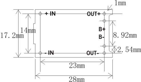
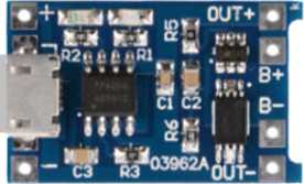
I’m struggling with this part and looking for a genius to create this part for me. I found a couple online but none are right. I’m using this charger board as part of a project, and need to place it on the pcb. I can’t find any technical drawings of this board so have done one myself. Please be aware that I have changed the pin spacing on the right to 2.54mm to match the header pin pitch. The real spacing on the actual board is 3mm but header pins with 3mm pitch appear like hens teeth to get hold of but as the board has 1mm holes it does fit onto 2.54 header pins.
Currently I have been placing standard header pins on the pcb and spaced them with the use of custom sized extra boards then deleted the board once in position. The problem with this is that I cannot group the pins and easily move them around to suit the board. So it would be better if a part could be created.
I can draw and save in vector format but the layers are the confusing part for me. I originally uploaded SVG files but changed them to JPG as you couldn’t see them. This is the breadboard SVG.
Your breadboard is missing the connectors and (as you noted) the layer ids. Your best bet is to start with an existing part (in this case either a similar power supply or a generic IC with 6pins. Doing that will get you the necessary layer ids and connectors to move around in the svg editor of your choice. I’ll clone something and upload a better part in a bit.
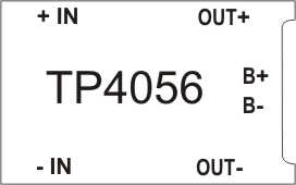
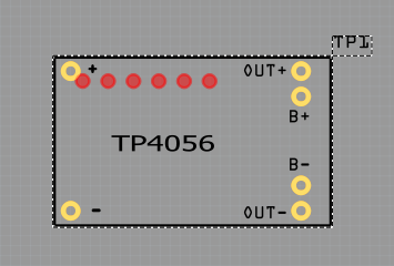
edit: OK its a bit later now. Below is a mostly working part as an example. I used copy / paste on breadboard to copy in 6 appropriate terminals from one of my other parts (DC 3.3v-10v TO ± 12V Mini DC converter.fzpz, posted here earlier). I changed the font from arial (which fritzing doesn’t support) to OCRA, but fritzing apparantly doesn’t like the tspan text either. You will need to find a working part breadboard and adjust the text xml til fritzing is happier. For schematic (and to create the fzp file) I used a generic 6 pin ic and modified the schematic. Feel free to move it around if you don’t like it. For pcb I copied in the pcb svg from the converter and changed the text so the pads match the connections in the fzp. You will need to move the pads and silkscreen around (leaving the grouping as is) to match the real board. To get the fzp and svg files just unzip the .fzpz file below (I use 7zip). If you have questions or problems please post. Note it is most useful to upload the fzpz file for the part (7th button from the left in the reply menu) as then we get all the files to look at.
Thanks Peter. The font is not important so whatever works. The pcb view is the important part. The schematic and breadboard are secondary to what I’m doing. It’s getting the pad placement correct that seems to be the issue. As I said originally the pad spacing is not the same as the actual board. I am using pin headers to mount the board to the pcb as standoffs. So have used 2.54 mm pin headers rather than the 3mm which would fit the board. Hope that makes sense.
The pads on the pcb supplied are set to a hole size of .038 in which fits the .1 headers so if you move the pads to the correct places and change silkscreen if you want to, you should be good. I need to poke more at why changing the font family didn’t fix breadboard but I haven’t yet.
edit: A replacement part where breadboard has correct text. I had to remove all translates, and then all the tspan text and pxs from font-size to get here and I’m still not sure why, but this is at least better and I have broken and fixed files to ponder …
Fritzing is not letting me load your new part as it is saying it is already loaded. I tried renaming the file, but it seems to be using an internal ID.
Thanks Old Grey but I have tried that and Fritzing is still saying there is a part loaded with the same name. So quite where it is hiding I don’t know.
I’m not sure but the problem appears to be that the name of ID is the same as the Battery Holder Peter did earlier, and that is in My Parts. While I have moved it out of the folder User, it still is in Fritzing somewhere as it is still showing in My Parts. I can’t edit it, but I can use it still.
Managed to do it. I have tried to edit the pcb SVG in Inkscape, by downloading it and editing it, but then when I resave it all the layers seem to have moved around. So it would not reload. This is the SVG I have redone and moved the pads and labels around. I had to resize the board as that was wrong, but now should be correct. As I said earlier the pad spacing on the right are 2.54 mm and not 3mm which would be more correct for the actual board. However I am using the part to place the holes on my pcb and the attachment will be by pin headers.
The correct way to remove a part is remove it from the bin inside FZ, otherwise you have to search and chase instance inside the file system.
Yeah you didn’t follow the FZ layer rules for PCBs. Go watch my PCB video if this doesn’t make sense.
You make a group called silkscreen and put all lines and text in it.
Make a group below that called copper1(top copper), and in that make copper0(bottom copper), and in that put all contacts. With round contacts the OD is the size of the pad, and the ID is the size of the hole.
If this part will be fitted to a custom PCB that you are making, make the header pins 3mm apart and just install individual pins in each hole.
Many thanks for that. It’s starting to make sense. I think I have the right layers, but when I change one layer it seems to change others, so seem to have got myself in a right muddle. Could someone look at this SVG and see what I have done?
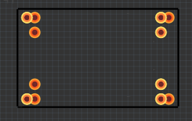
Thanks for that Old_Grey, but somehow the connectors seem to have stayed where they were and not moved with the copper layer. Not sure what layer they are on? Here is an image of what comes up when I load the part. Any ideas?
I managed to get the connections sorted but the fonts suddenly went really small. Also I added the part initially to the top layer of my pcb, then rotated it 180 degrees and moved it to the other side. The connections all moved correctly but the copper pads stayed where they were, so I ended up with two lots of pads.
Your one worked sort of. Top view it loaded properly. Then I rotated it 180 degrees and moved it to the bottom at which point it reverted back to a 6 pin generic header. So I tried it by moving my view to bottom and then added the board. It worked no problem and didn’t have to rotate it. Why it is doing what it is doing is beyond me, but for now it’s working.
See the px
font-size:1.57729566px;font-family:OCRA;fill:#000000;stroke-width:0.42061219
Remove the px
font-size:1.57729566;font-family:OCRA;fill:#000000;stroke-width:0.42061219
The part above has been fixed for fonts and works fine. You can get the svg out of that if you need it.
 I originally uploaded SVG files but changed them to JPG as you couldn’t see them. This is the breadboard SVG.
 So I tried it by moving my view to bottom and then added the board. It worked no problem and didn’t have to rotate it. Why it is doing what it is doing is beyond me, but for now it’s working.