Hi, I would like to use an SVG image as a logo for my PCB. I already created the SVG (on https://www.figma.com) and when I open the SVG file in the browser (Chrome) I can see the image correctly.
However, when I import the same SVG image on my PCB as a ‘Silkscreen Image’ on the top layer of my PCB the only thing I can see is a blacked out image
When I move the SVG to the bottom silkscreen of the PCB, I can see the image slightly. This is the correct image, but on the bottom silkscreen.
Is there an extra step I have to make to load the SVG correctly? Do I need to convert my SVG to a PNG file? If so, how can I keep the image quality?
The link doesn’t lead me to an svg file. If you rename the svg file to .fzp (the forum often has troubles with svg files) and upload it here I’ll have a look at it. There are a variety of posts in the forum on logos (usually on copper rather than silk though) and it is picky about paths (I think the gerber code has bugs). Most of the people with expertise in this area are no longer active in the forums though.
edit:
Please upload the .fzz file of the board you want the logo in as well as the logo svg.
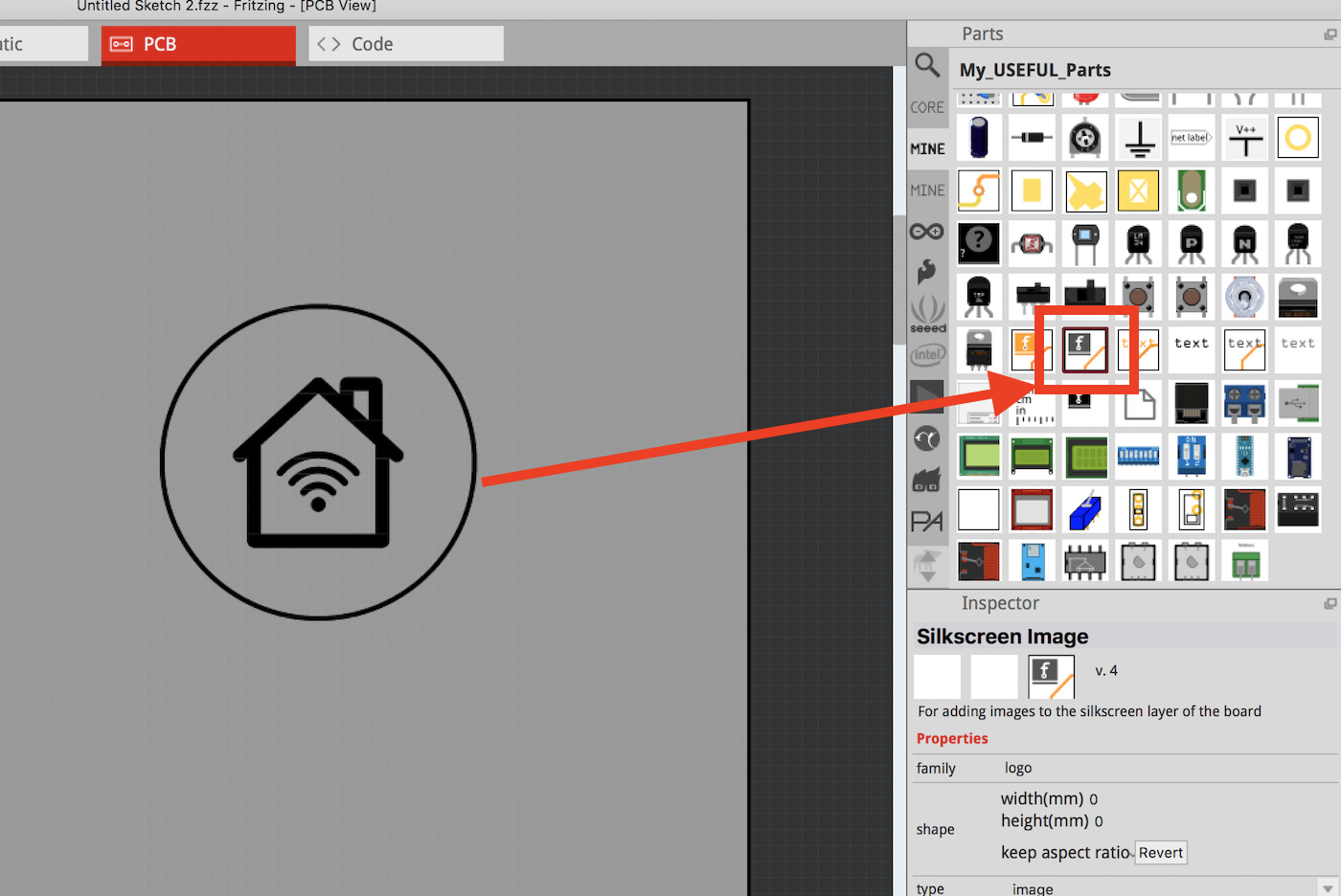
I don’t think you can do the logo as it stands. There is only one color in silkscreen. You are getting the black circle as the white circle under it all is changed to black. The rest of the outline disappears in the black of the bottom circle. You can print the white house and wifi bars as silkscreen which will be over the board color, but thats all. Silkscreen won’t do additive or subtractive layers as you have done in the svg. If you are good enough at path creation you can create a path that matches the black areas in the logo (as a single path) and use that as the silkscreen and that should work. I’m not that good at paths, so I did this instead (by deleting the circles and changing the path to black which Fritzing will do anyway) then adding a circle around the paths. This is constructed as a part because I thought I didn’t know how to properly format the svg (and I still may not) before discovering what the real problem was when I made it a part. I also shrank the scale of the svg to be somewhat compatible with the board as I don’t know how the load mechanism handles scaling. You may want to leave it as a part because I’m not sure you can move the logo around, it may be fixed in one place, a part you can drag around as you like.
You can load the fzpz file and it will put a part called logo in you mine parts bin. Dragging it in to pcb will give you the logo (and a part label that you need to hide by clicking on it and hitting hide.) Its size can be adjusted in the pcb svg for the part. Here is an image from pcb I have not hidden the part label in this one:
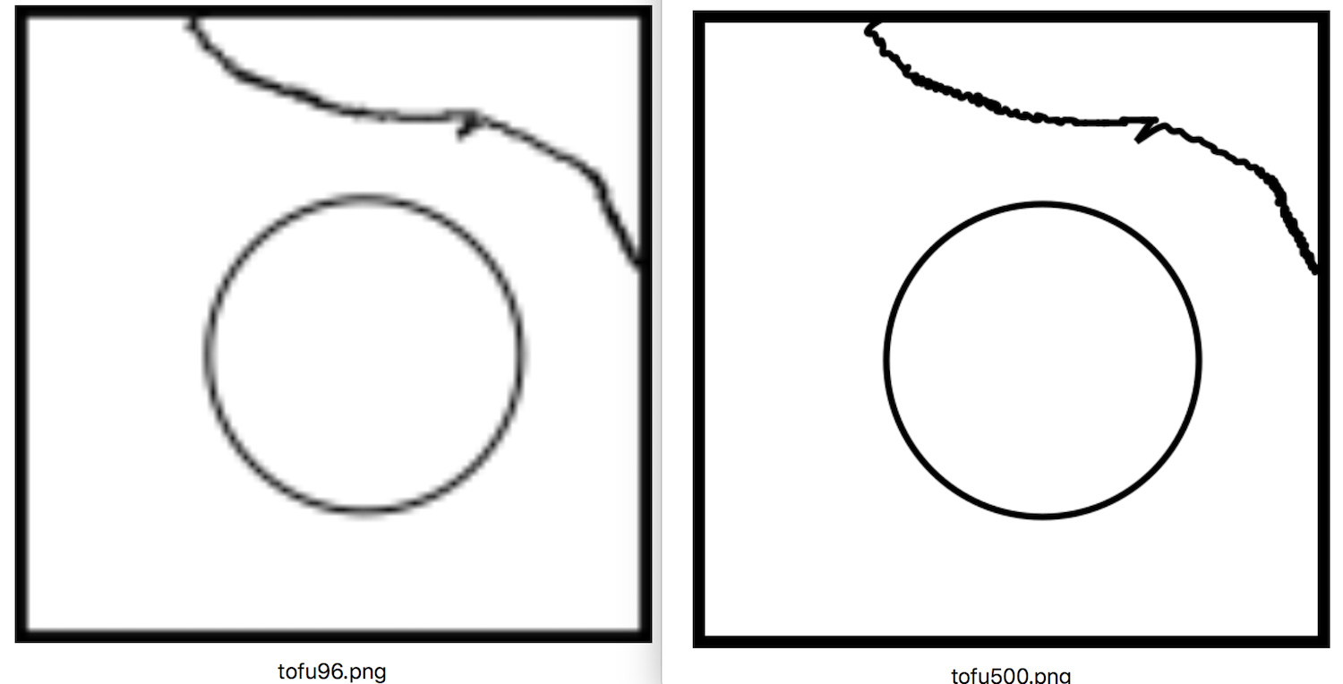
However it still needs work as gerber processing doesn’t like the path:
It isn’t worth pursuing at this point until I know what you want to do with the logo. It is entirely possible that converting this image (with the path corrected in some undefined manner, I usually move infliction points until gerber is happy, I think there is an overflow problem somewhere in gerber processing) will work with logo loading with a properly formatted svg (it needs 3 groups each with a copy of the image in it, labeled board, silkscreen and silkscreen0).
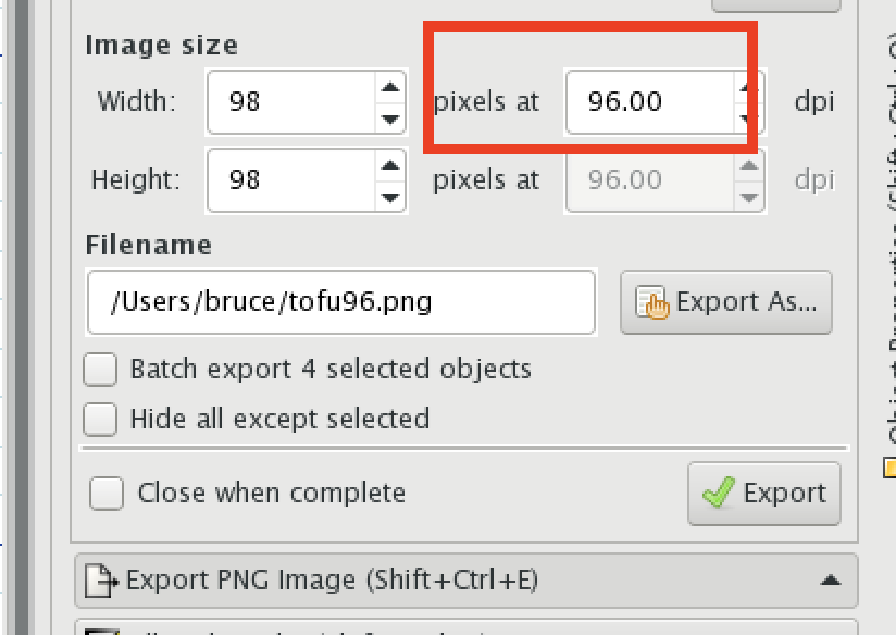
I must have missed something in reading the posts - For some reason I’m still thinking what’s called for is simply using the Part called “Silkscreen Image” and (here’s the trick) - to succeed, the image must be a .PNG, not an svg.
I changed the Silkscreen image so it loads a PNG file now, instead of an SVG file.
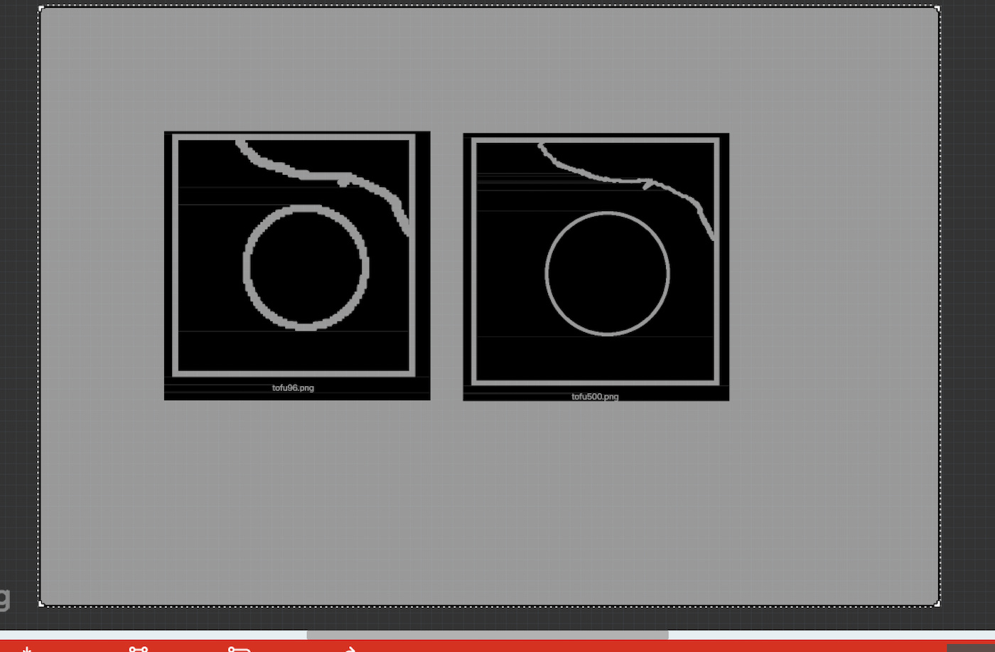
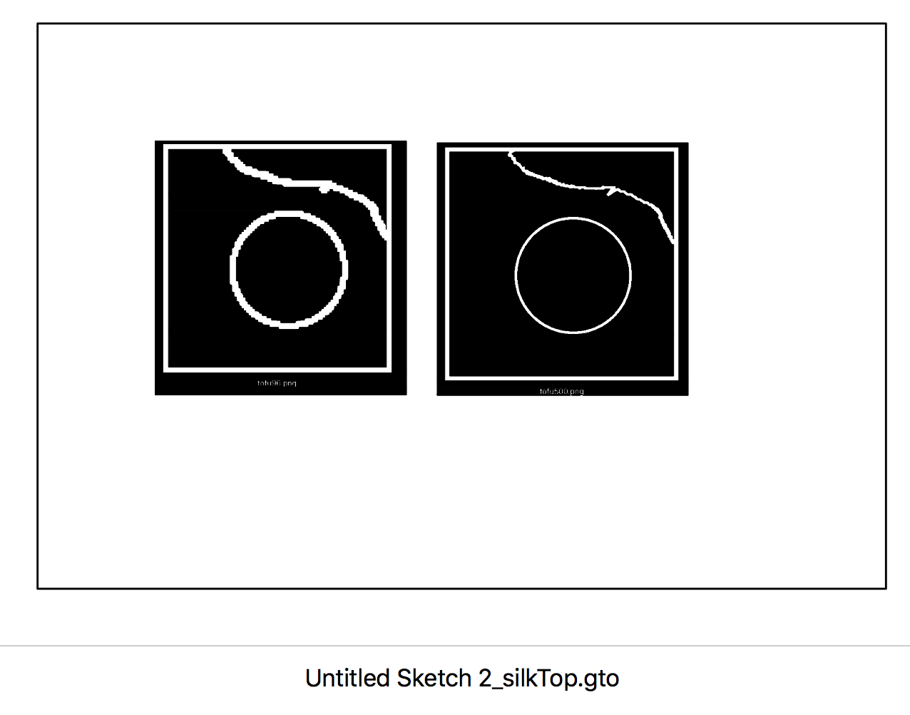
I have exported the PCB as a gerber project. If I open the gerber layers in some gerber viewer (Gerbv in this example) I can see the image in low resolution. How would this affect the actual PCB print, does anyone have any experience with that? I think the image is fine like this to send the PCB out for production, right?


