I have a serious problem. I had designed an entire PCB around a QFN-24 pin (3.5mm x 3.5mm) layout on fritzing. But only on ordering the PCB i came to realize that the fritzing supports only 4mmx4mm and not the 3.5mm x 3.5mm kind. I am facing serious trouble here since, a small mistep is causing a huge problem when it comes to soldering the chip. Is there a way to create the 3.5mm x 3.5mm version in fritzing . I tried looking at all available parts but it does not seem to exist. Could someone help me to find it? or how to modify it?
Given the data sheet / package foot print it isn’t a big deal to modify a footprint and make a new part, but as Old_Grey said we would need a data sheet. Google finds references of a sort to qfn 3.5mm but it seems to be stencils and implies a .4mm pitch (but all the package outlines I can see are .5mm pitch) so the chip and package datasheet that you need are the first step.
The exact chip name is XR18910. Its a QFN chip with 24 pins
Here is the documentation http://www.mouser.com/pdfdocs/XR18910.pdf
. The dimensions are 3.5mm x 3.5mm. Could you help me find a way if there is a way to modify the existing 4x4 mm QFN-24 pin chip to a 3.5mmx 3.5mm QFN-24 pin chip
Here is the data sheet. http://www.mouser.com/pdfdocs/XR18910.pdf . The footprint of the part is available in the PDF. It is extremely similar to the .4mm variant. I just need to reduce the size a bit. I do not know how to do it though. Could you kindly assist me here?
The package is called tslp by Exar. Below is what I hope is an appropriate footprint (as Exar only has the package footprint not a recommended pcb layout, not does anyone else I can find). I took the ITG-3200 (which I assume is what you used as the base of your part) qfn-24 4mm footprint and reduced it to .4mm pitch .24mm pad width (pin is .2mm nominal ± .05) and .6mm long. extending .2mm outside the 3.5mm package boundary (because that is what the 4mm part does more or less). You should be able to replace your parts current pcb svg file with the one below (it is really a .svg renamed to .fzpz so the forum will upload it, it doesn’t always like svg files) and copy it over your current pcb svg file either from the command line or via parts editor. You likely want to print a copy of the footprint and check it against one of your ICs to make sure I got it correct though .
edit: not quite right yet. Fails drc on overlap and some connections look wrong. I’ll have a look and upload a corrected version. May have to reduce the pad width to get by drc. Turns out to be mostly a false alarm. The original part doesn’t use all the pins, thus they aren’t all active and the original foot print also fails drc so I guess we live with that. I did however update the above file as I reduced the pad width from .24 mm to .22mm to increase the inter pad distance by a whole .02mm (but every little bit helps ). the pin is .2mm nominal ± .05 so there is .01mm either side of copper. In addition I noticed that the center pad is a heat sink and is 2.2 mm square. The current pad was only 1mm square, so I increased it to 2.2mm. Post if you have questions. Feel free to upload your sketch and we will check it over for you. Please tell us if the footprint works, if so we can add it to the library.
Its helpful in so far as they think a .2 mm inter pin spacing is ok, and mine (in the latest one) is .18mm so may be ok. When we get down this far I don;t know where the limits are … There seems to be a real lack (or I don’t know where to look or what to search for) of information on the 3.5mm package. There are stencils and adapter boards that show up but no foot print examples that I’ve found and not many ICs (and those are like the Exar, show the package but not a pcb footprint).
It may help to know that most prototyping board places (cheap low quantity board fabrication from china) say a low limit of 6mil spaces and 6 mil traces but they prefer 8mil spaces and traces. Once you go to pro boards (4 layer plus) you can go down to 2mil but they again prefer 4mil.
I have my DRC set to 8mil and will go to 7mil when I have no other choice.
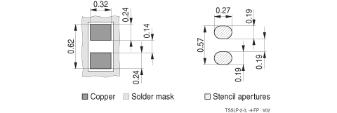
With the 0.5mm pitch 0.2mm pad they use a footprint of 0.3mm pad with a 0.2mm gap, and if you Image search TSSLP the smaller ones are 0.24mm pad with a 0.14mm gap, and going by general PCB manufactures they don’t like smaller than 6mil or 0.15mm stuff.
Thanks, 6mil is .152mm and 8mil is .203mm (so a little larger than the inter pin gap on this footprint at .18mm) so I look to be right around the border line, but at least it should be doable even if he has to beg the fab house . I’m just glad I don’t have to place and solder this thing, the pins are under the chip (although my footprint extends out a whole .2mm past the edge:-) ).
You are just amazing. Im actually trying to get my current build recitifed. But im facing certain difficulties. I have uploaded my fritzing data here. The component im trying to replace with is the one i show below. But im unsure if i have to redo the entire circuit or if i can simply replace the component footprint with your footprint, the one used in the PCB design file attached below was the 4mm one. I am going to be hand soldering it either with a heat gun or some SMD soldering tricks. I have done it before using a heatgun and soldering iron on breakout board. but this being a 4mm version i was not able to solder it. i wish to rectify it. Would you have advice?
Download Van’s .fzpz file.
Change the .fzpz extension to .svg.
Right-click IC and select Edit.
In PCB - File/Load image and find the now .svg labeled Van part.
Click on the pin labels in the top right box and make sure the correct ones highlight in the drawing.
Go to Meta and change the Properties from QNF to TSLP.
File/Save as new part, and add a -2 to name.
Close Edit.
Close fritzing saving the bin.
Open FZ and select part, and in Inspector select package TSLP and it should change.
Thank you old grey. I used the part that vanepp sent me. And i think its look good for now. I will send it out for fabrication. Fingers crossed that the chip will solder well onto the board. Thank you so much I have attacehd the PCB to show how it looks like
You have to reset the grid and straighten the traces.
Be 100% sure that it’s right, as there is no use doing it wrong, by checking the Gerbers. There are online Gerber viewers, or you can use the free Gerbv, or even print it out and check it.
Thank you Old_Grey. This time i printed out the circuit onto a PDF just to see if it somehow aligns to the chip i have. It seems to be more or less accurate :).
If you are going to hand solder this, then I’m glad I was lazy and left the pad width at its current .22mm instead of the .3mm recommended in the Infineon part. While it will make placement a bit more tricky there is a touch more space between pads to avoid solder bridges. I see you have connected the heat sink copper on the bottom of the chip to ground which is probably a good bet. The data sheet calls it pin 0 but doesn’t show it as connected to anything, so it shouldn’t mind being ground. Good luck, and tell us how you make out
edit: Looking closer at the gerber output with gerbv, you may want to straighten the connections in to the thermal heat sink. They both bend a bit from the vertical and thus reduce the spacing between pins. Same with many of the other connections in to the IC pads. Given the distances I think you want as much separation as possible to avoid solder bridges (although the two on the copper pad are probably the ones most at risk as they will be under the chip and not accessable).
I’m not sure if Van’s 0.2mm extension to the pad is enough, but if the pad protrudes past the body of the part you might be able use a soldering iron and wick the solder under the chip. Then just put a via in the middle and wick it to the center GND pad from the other side.
By the sound of it he has the solder paste sorted and just heats it with air.
 .
.

 . I’m just glad I don’t have to place and solder this thing, the pins are under the chip (although my footprint extends out a whole .2mm past the edge:-) ).
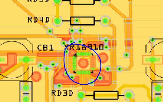