OK, took a while and is quite long but here is a fixed part and what I did to fix it.
breadboard svg:
edit in Inkscape
ungroup by selecting the top group and pressing cntl-g until there are no more groups. This removes all the groups and most transforms.
Problems here:
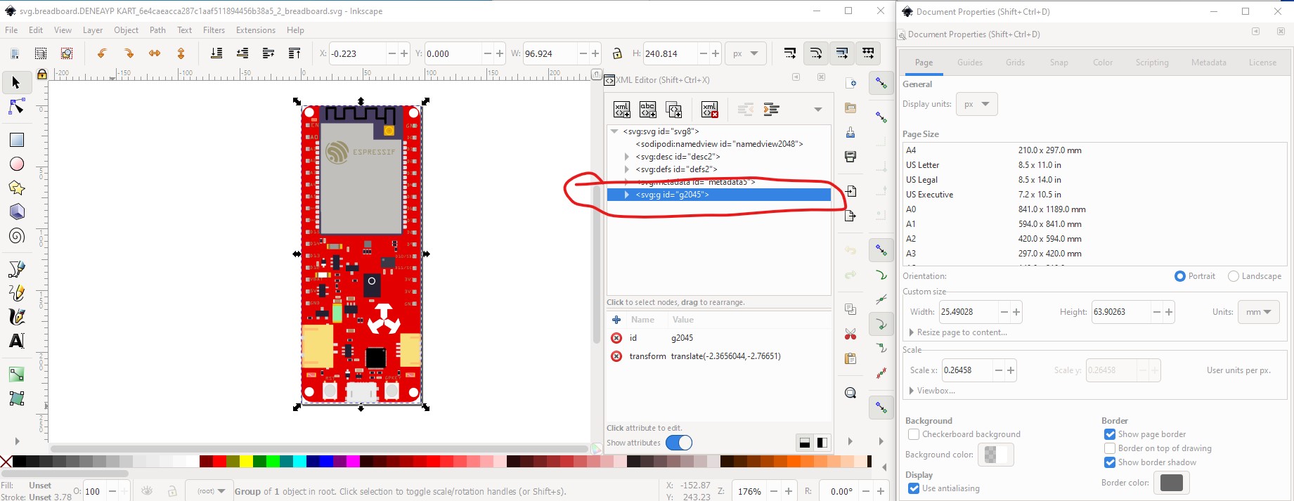
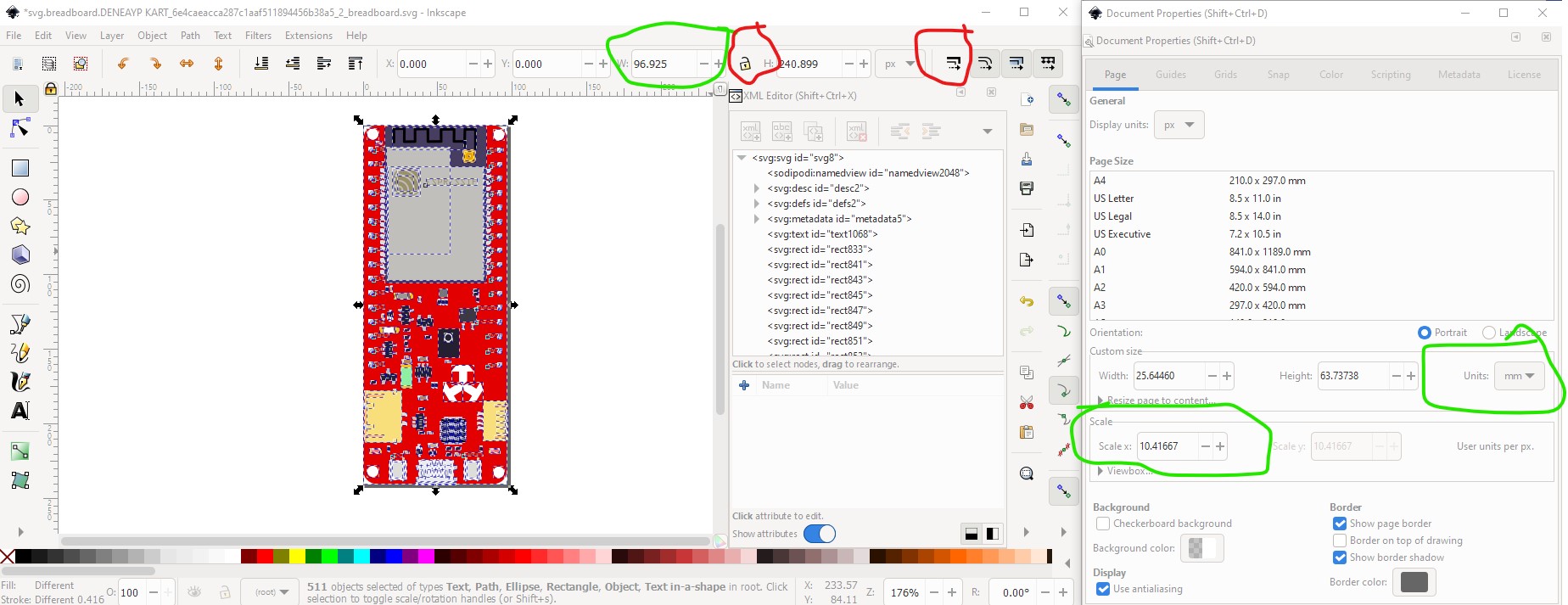
Edit->Select All
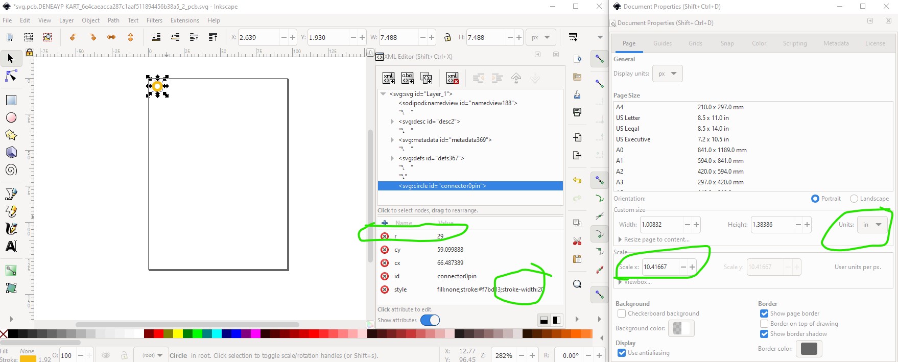
The start coords are not 0 0 (red circle in on the top tool bar) and the scale is not 10.41667 (red circle in Document Properties in the left window.) The document units are mm (which is fine, but the scale is different so I changed to in!) circled in red in the Document properties window.
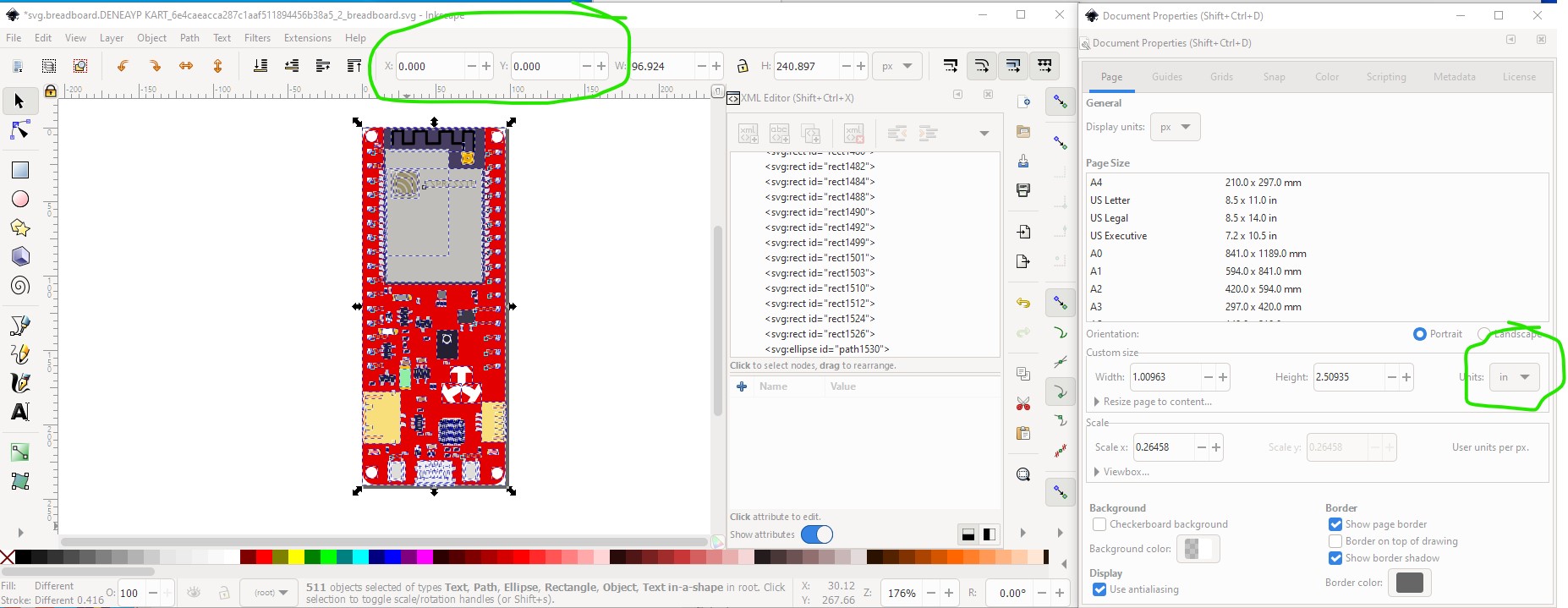
to fix the non zero starting coord
Edit->Select All
Edit->Resize page to selection
which changes the coords to 0 0 and rezizes the viewbox.
Then rescale the image from the current 0.26458 to 10.41667 which will give the desired 1 drawing unit = 1 thousandth of an inch in the viewbox. To do that insure that w and h in the tool bar are locked together, and Scale Stroke width is enabled then record the current width value of the svg (96.925px here.)
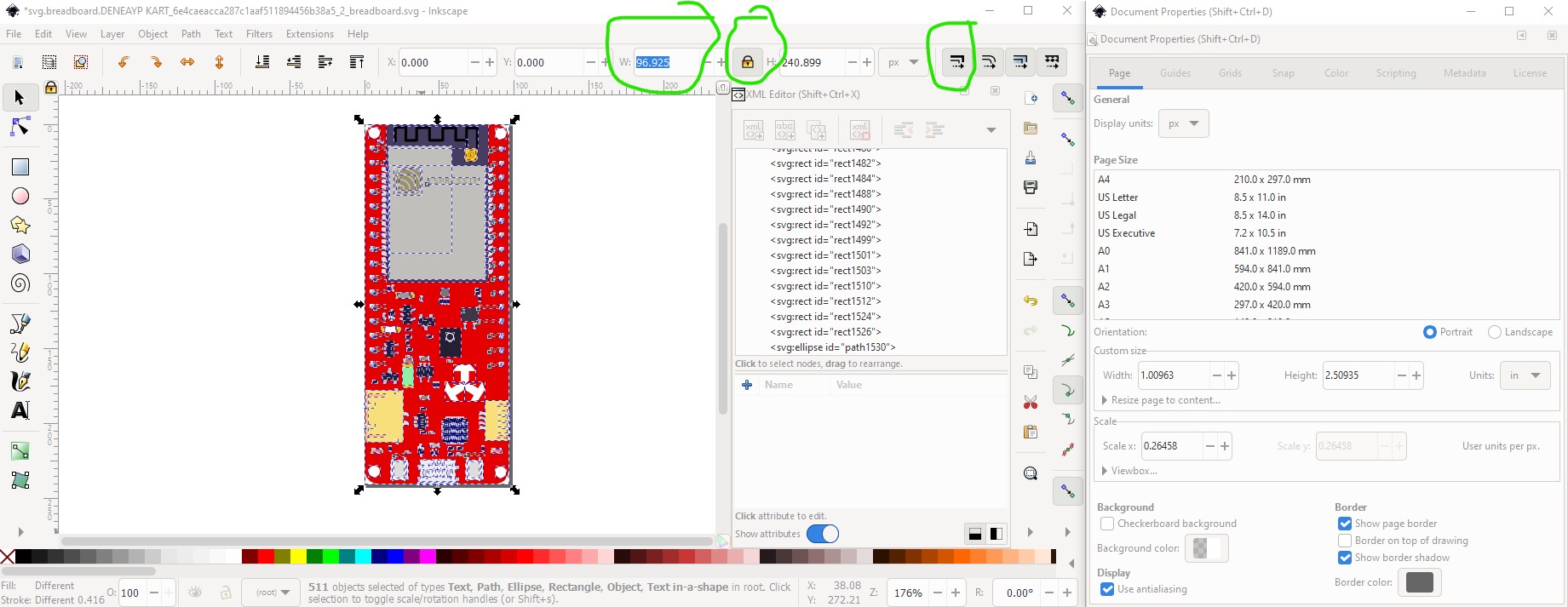
then change the scale from 0.26458 to 10.41667 and apply it. Which produces this:
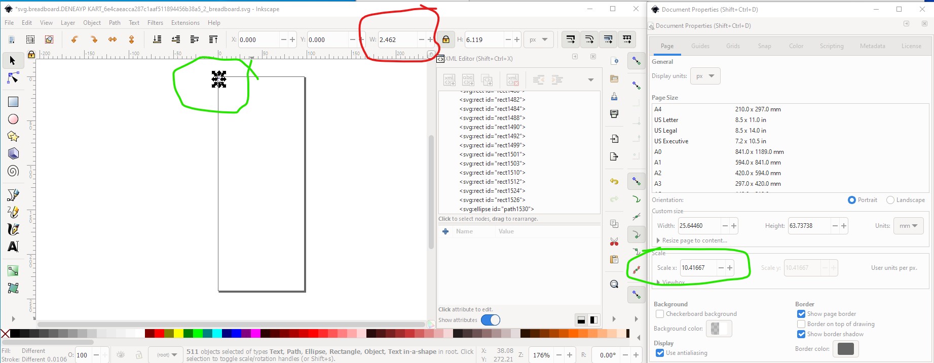
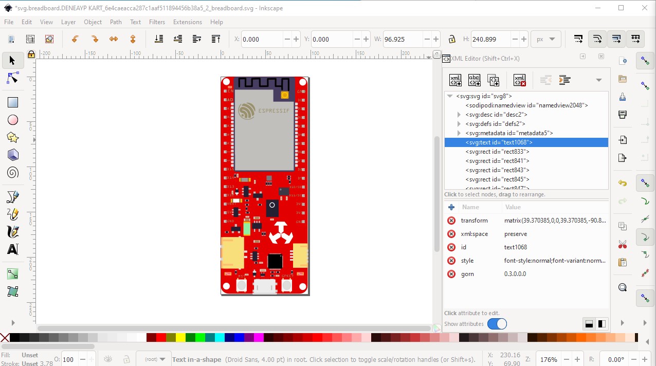
To restore the correct size to the image change the w in the tool bar back to the 96.925 value we recorded above which gives:
Here the scale and width (and because of the lock also the height) are correct. Now remove the lock and disable Scale stroke (circled in red) to go back to the normal drawing environment.
The first text element has no text and thus doesn’t do anything (it also doesn’t hurt anything) so delete it.
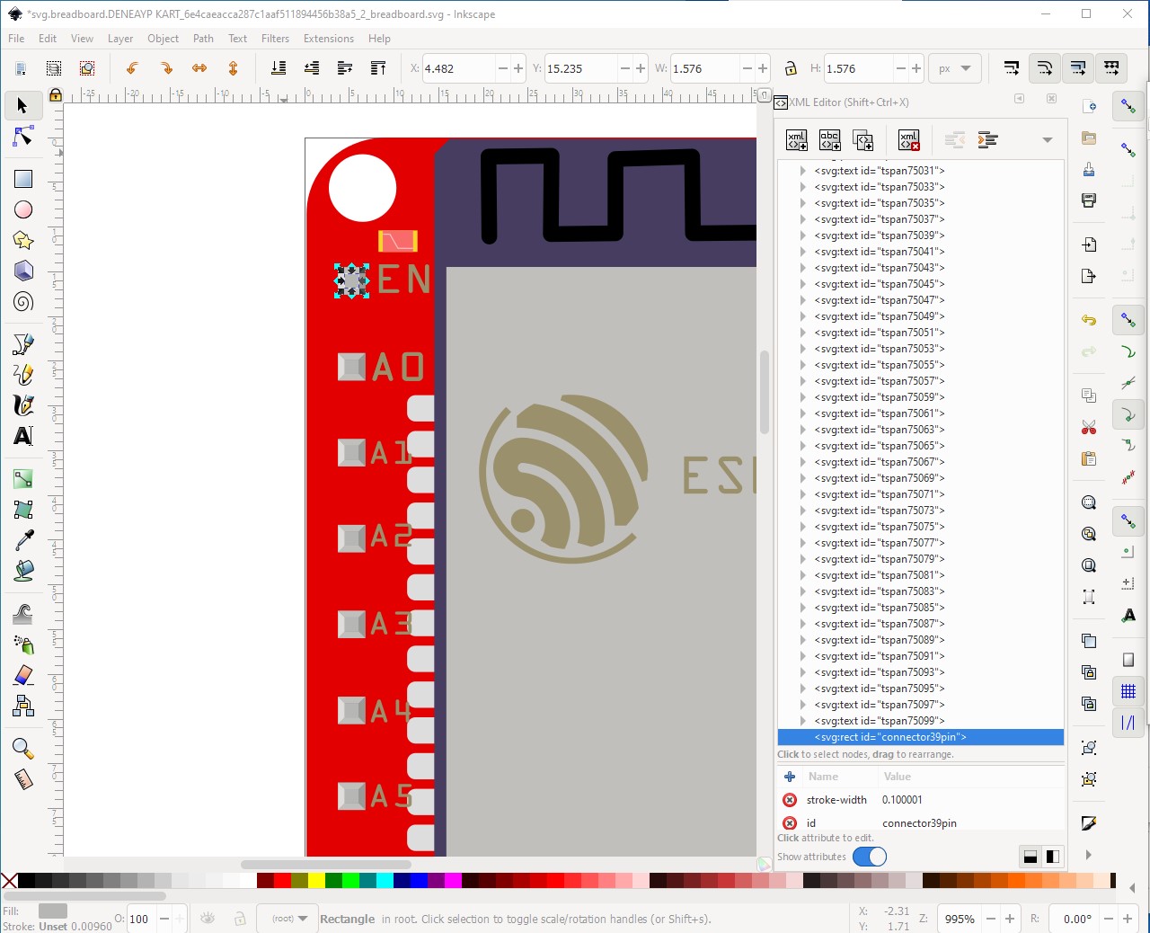
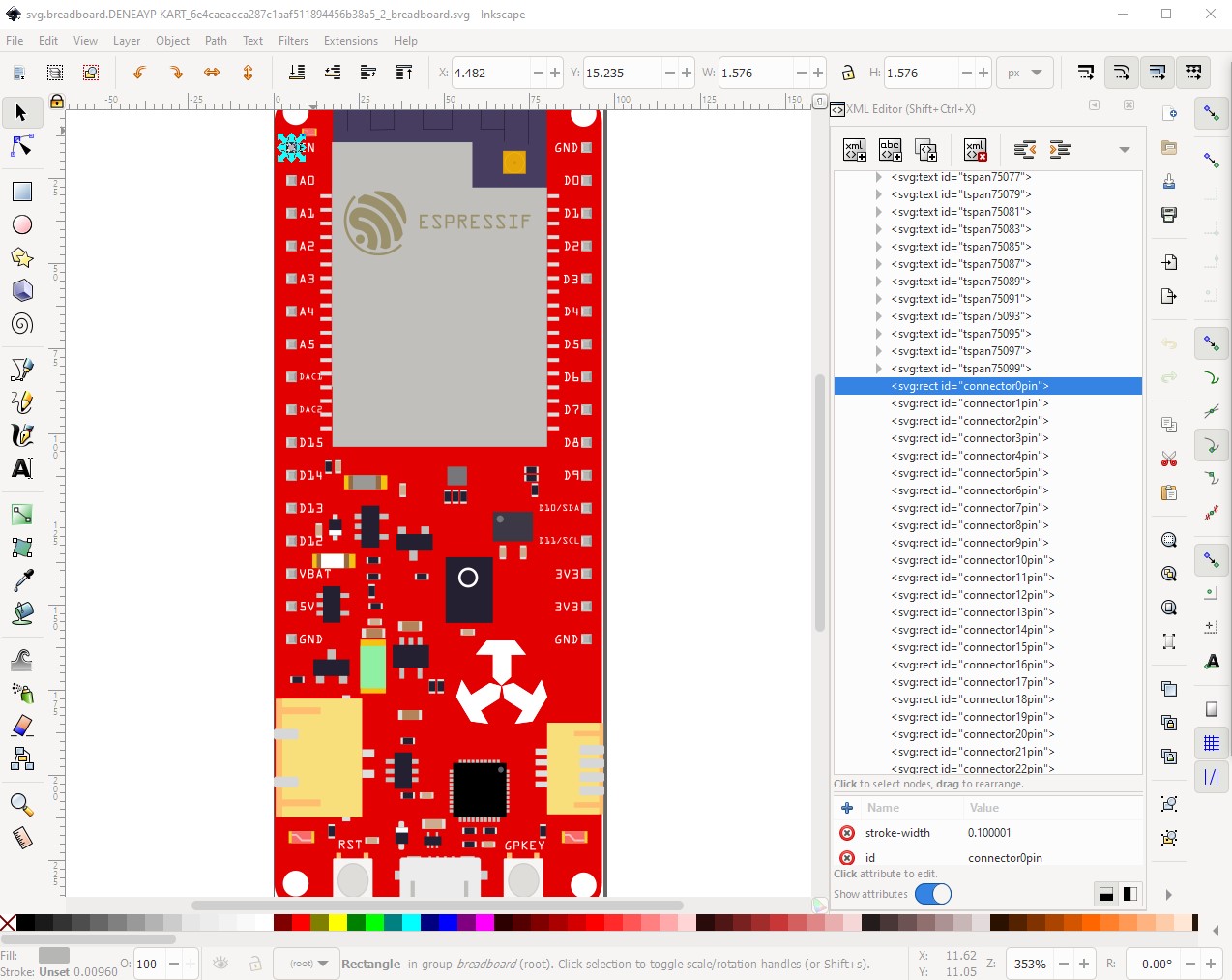
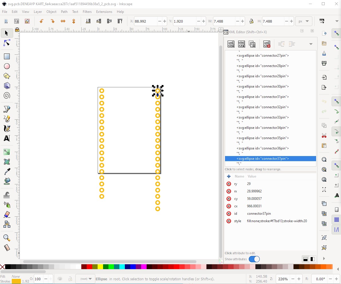
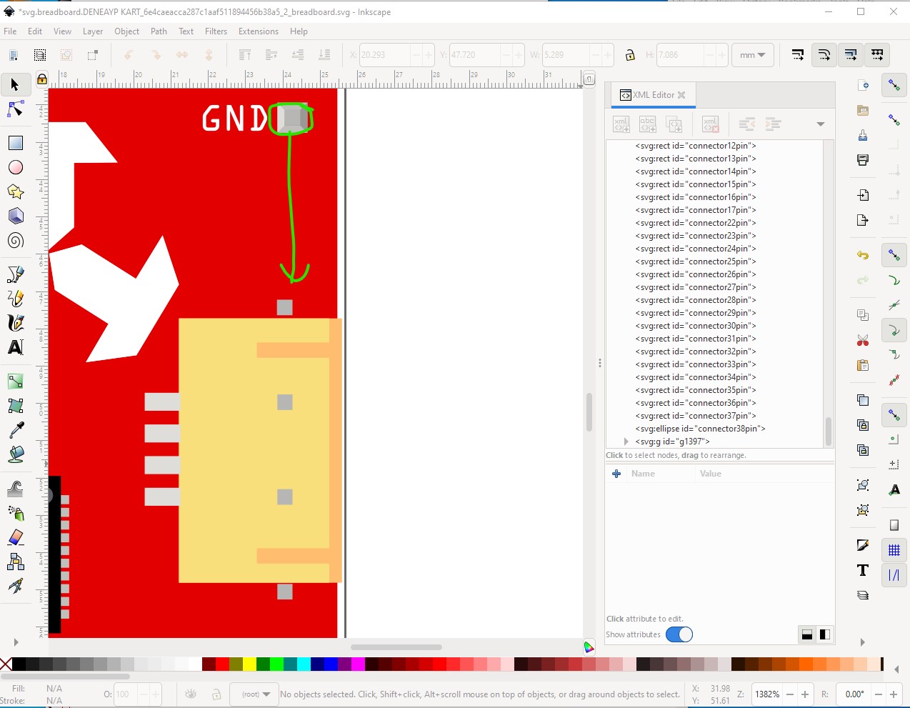
Now move all the pins to the bottom of the svg in order, starting with pin 1 at the top left of breadboard like this. First select the connector we want to become connector0
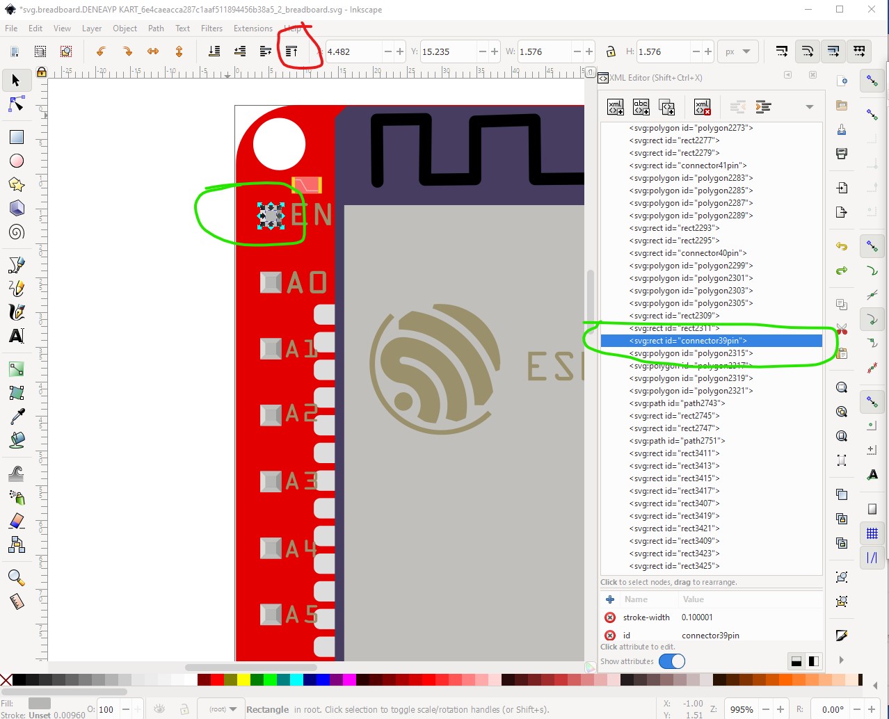
Then move it to the bottom of the xml window via the tool bar raise element to top (home) icon (circled in red here):
Do the same for all the rest of the pins in order til the svg looks like this:
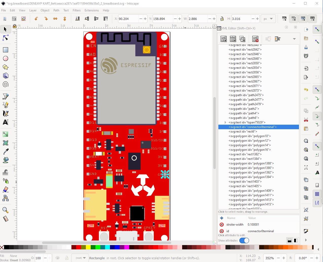
Then we move to the top of the xml window and do a search (cntrl-f) for connector which turns up connector0terminal instead of the desired connector39pin (which will be the new connector0pin.) So delete the connector0terminal element as unneeded.
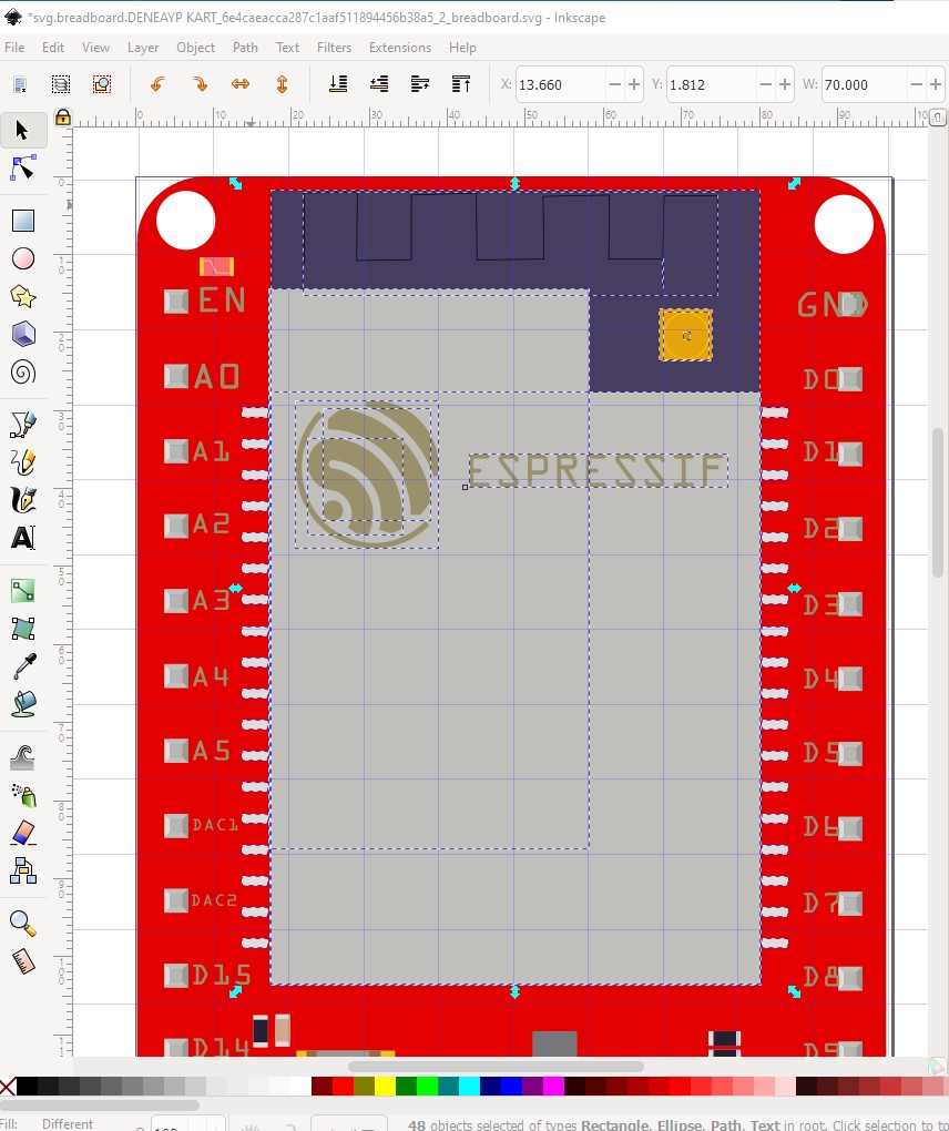
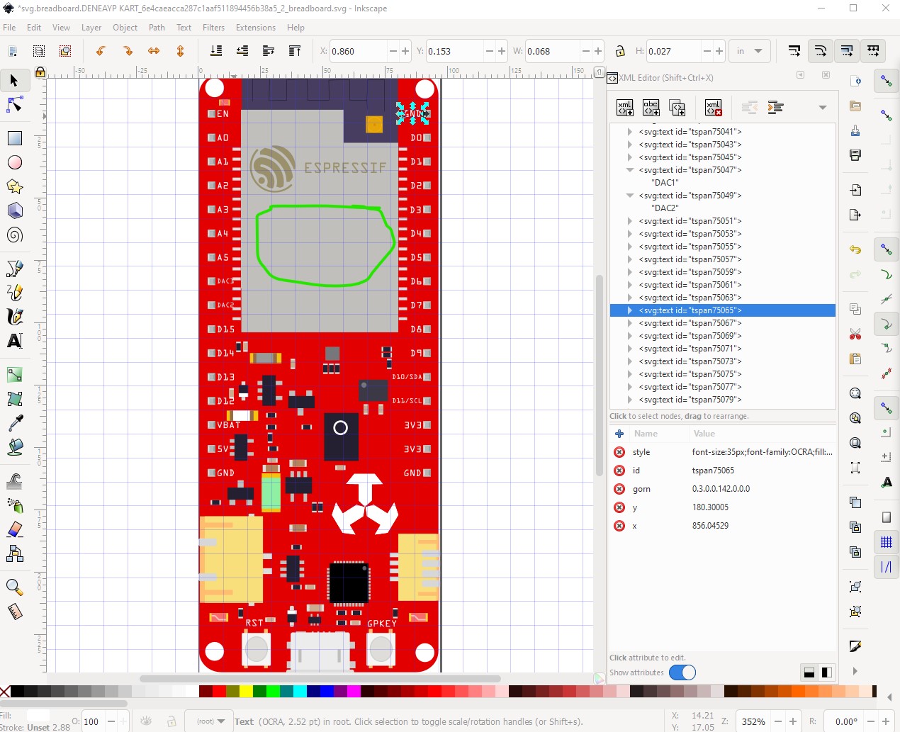
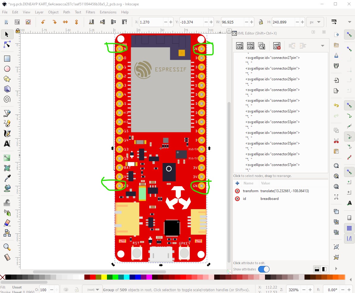
Now on to the text. Currently the text isn’t very readable (because of the color) and overlaps the pins. I’d suggest (and have done here, which you may want to change back!) to compress the esp module in X by a bit to open up enough room (with a smaller font size) to fit the text between the pins and the esp module. As well I’d change the color of the text from tan to white to make it more readable like this first select the entire esp module:
then reduce its width by a bit (3 px in this case) and recenter it in the board like this:
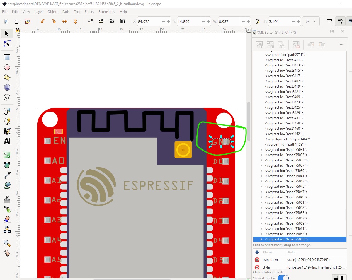
Then change the text definition so the font-size is 35px (smaller than it was), and the fill is white instead of brown to be more readable against the red background like this.
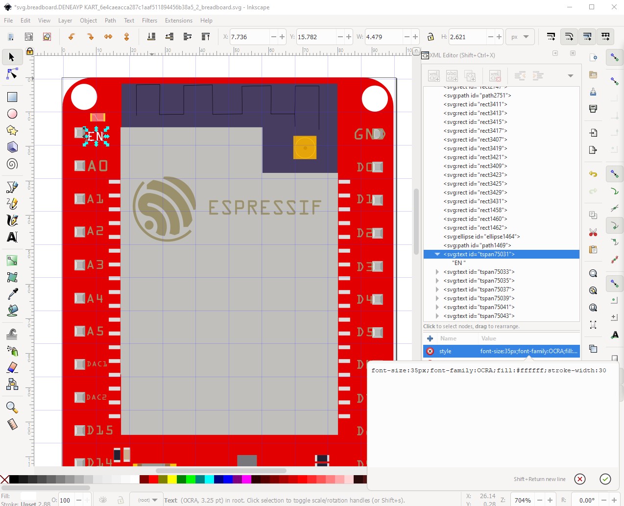
You then also need to move the text to be in the center of the pin like this. Note the new text is slightly smaller and white compared to the current text.
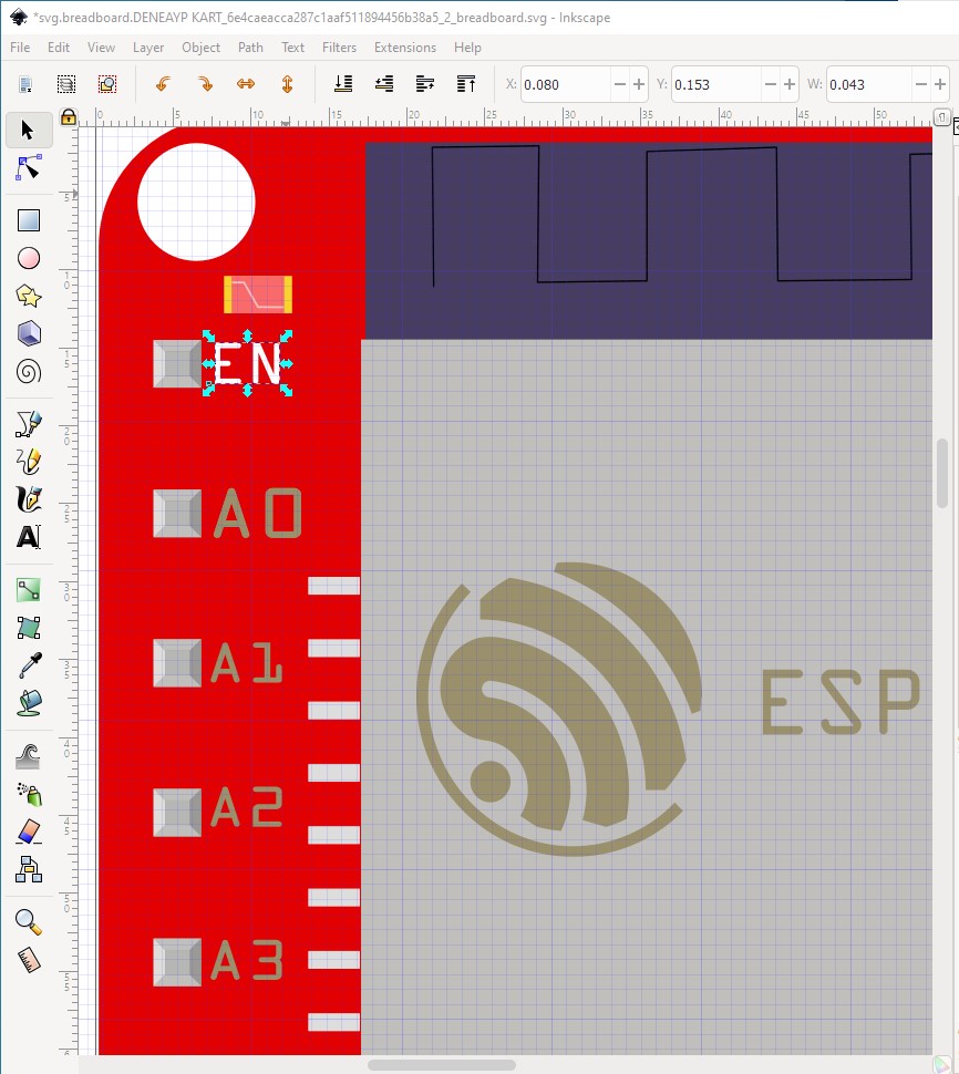
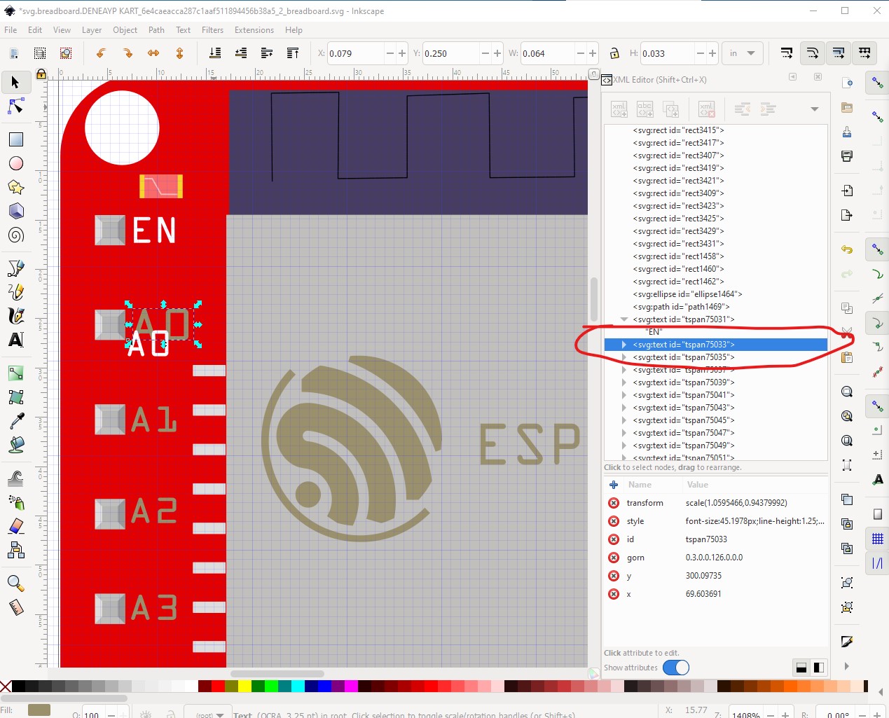
Now repeat this (using the same x coord and y coord + 0.1in) for the rest of the text. Note there are two copies of the A0 text, so delete the second copy as unneeded.
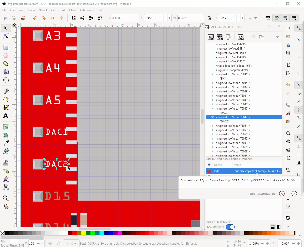
For DAC1 and DAC2 (which are longer than the others) I reduced the font size from 35 to 25 and adjusted the Y coord by a bit to center the text on the pin.
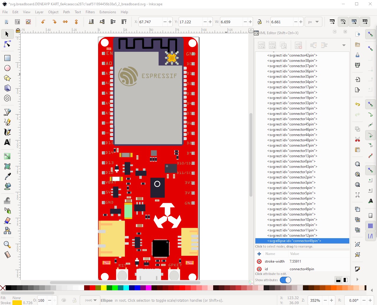
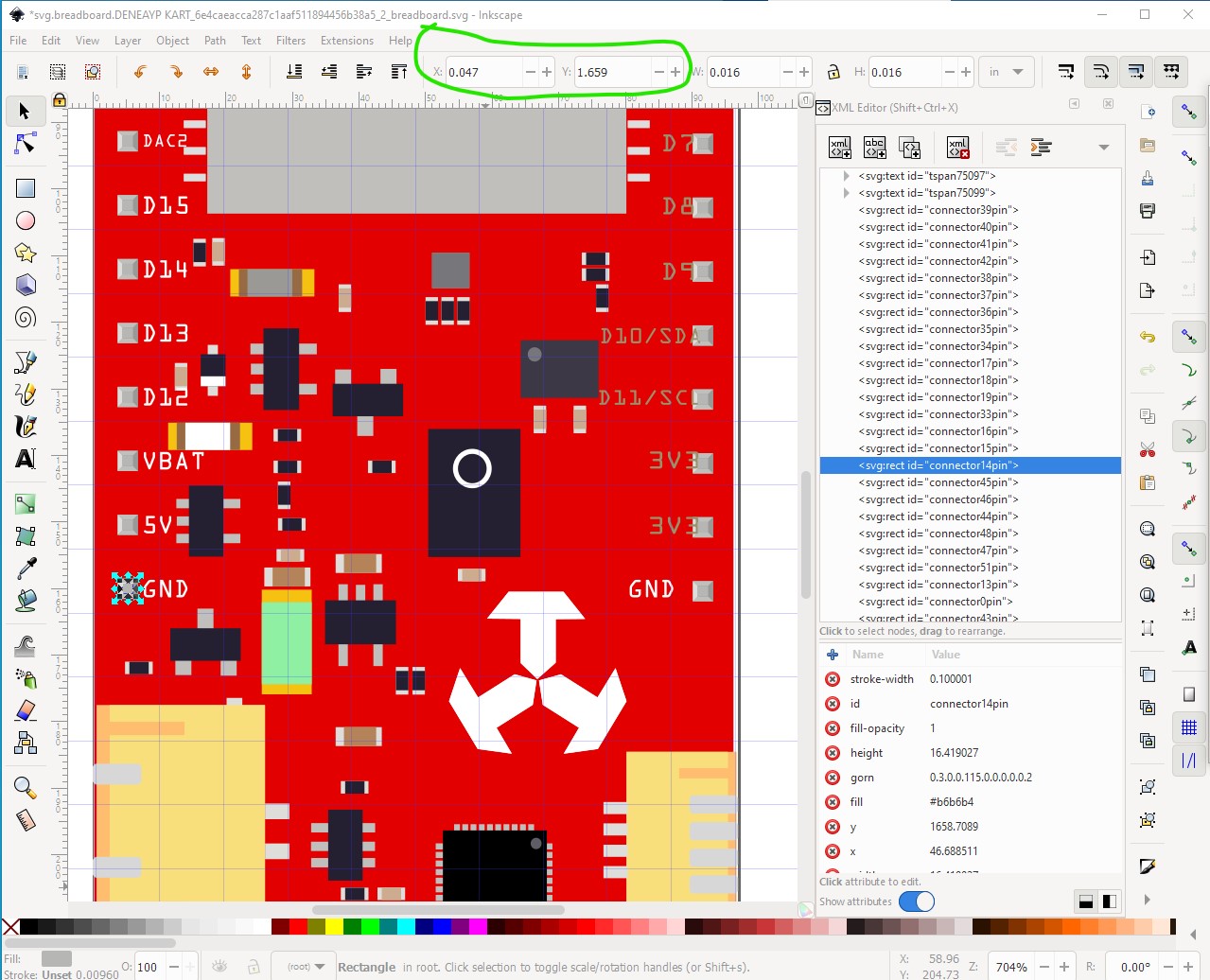
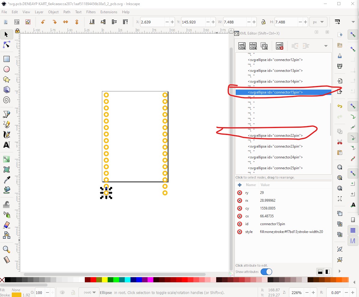
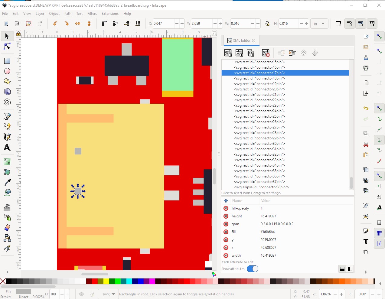
while doing connector14pin to connector13pin (on the opposite side of the board) I discovered that the pins are misaligned in both x and y. Here we have connector14pin with x 0.047in and y 1.659in (circled in green on the tool bar)
when I change to connector13pin on the right side of the board,
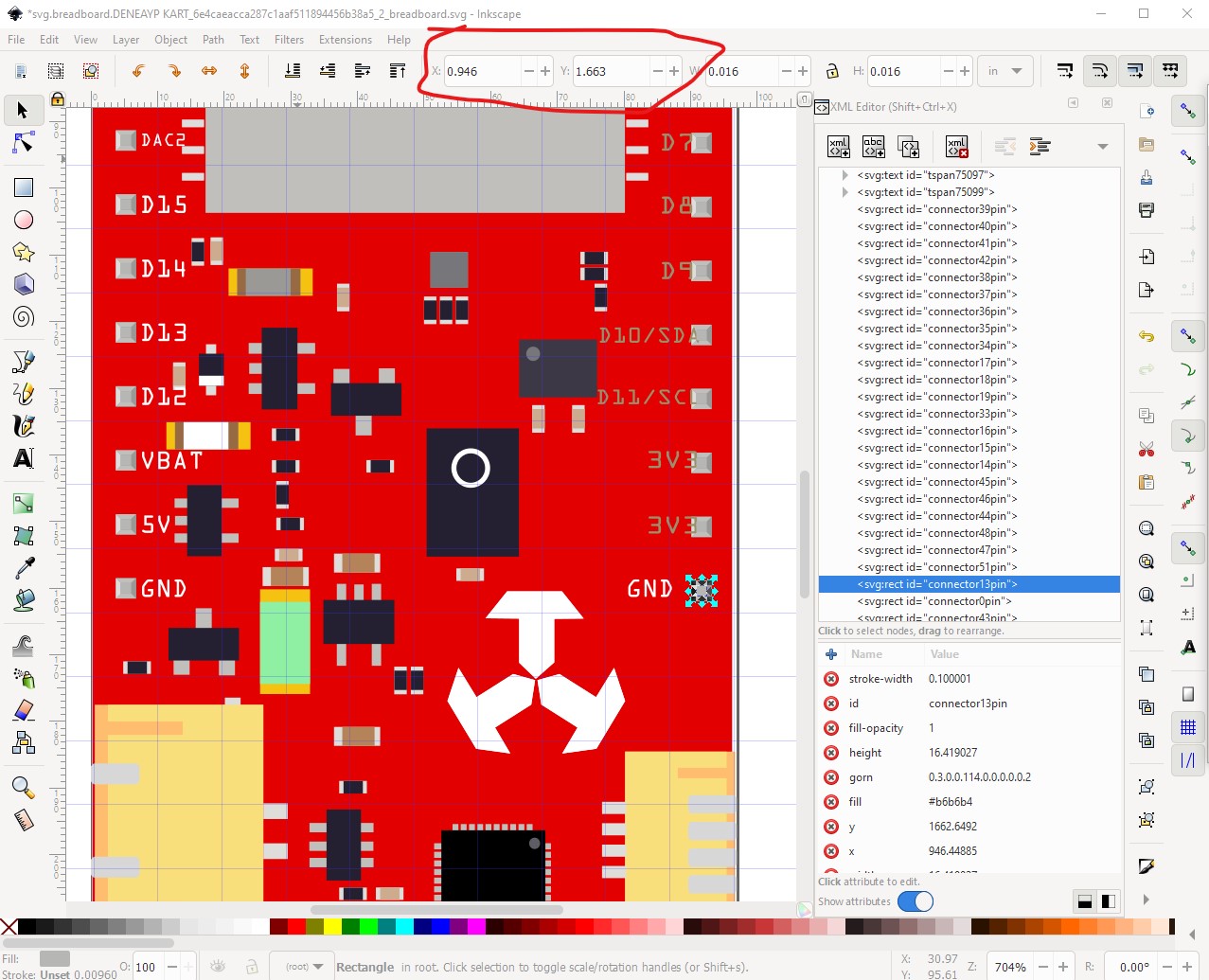
the x coord is 0.946 (and should be 0.947 to have a 0.9in pitch) and the y coord is 1.683 instead of 1.659 to match pin14. so select the entire column of connectors on the right of the board and move them to match exactly with the ones on the left side to be the correct pitch! Like this:
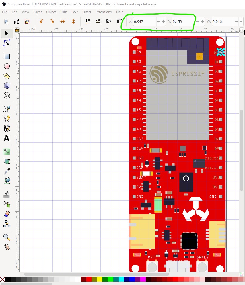
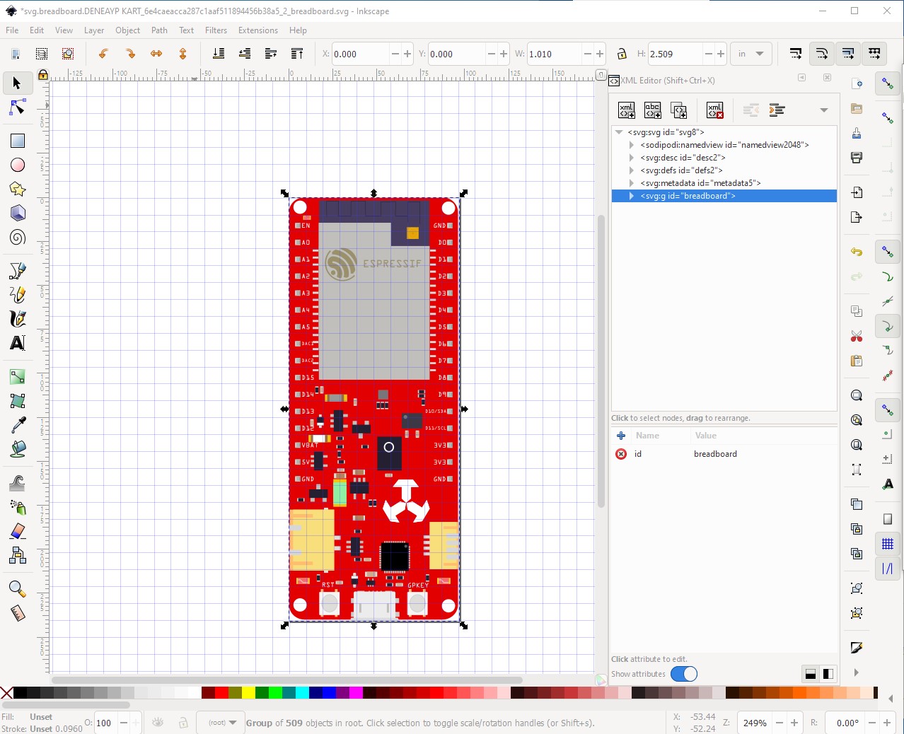
where the opposite pin is 0.9in larger in x and identical in y as it should be. Then continue changing and positioning the text until we end up with this which is the final breadboard svg (except for the pin numbers which we will do outside of Inkscape!) Note that you should add the model number (such as Wroom-b or Wrover-c3) to the esp module so the user knows which module is there. I don’t know what you are using so didn’t add anything.
At this point we are ready to do Edit->Select all, Edit->Resize page to selection and then Object->Group. Then name the resulting group breadboard and save the svg as plain svg.
Now it is necessary to renumber the pins in breadboard. In my case I have a python script which will do that like this:
$ SvgSetConnectorsbb.py ‘svg.breadboard.DENEAYP KART_6e4caeacca287c1aaf511894456b38a5_2_breadboard.svg’
*** Process svg.breadboard.DENEAYP KART_6e4caeacca287c1aaf511894456b38a5_2_breadboard.svg ***
which produces a svg that looks like this:
without the script the same effect can be had by manually changing the id field of each of the pins to the correct name (starting with connector0pin and going up by 1 for each pin) in either Inkscape or with a text editor directly on the svg file. There is further work needed on my script before it will be ready for release.
which is the final breadboard svg where the pins are numbered in sequence starting at connector0pin. Now we need to modify the schematic and pcb svgs to match breadboard (in practice we will recreate both rather than try and use the existing svgs) then modify the fzp file to reflect all the changes.
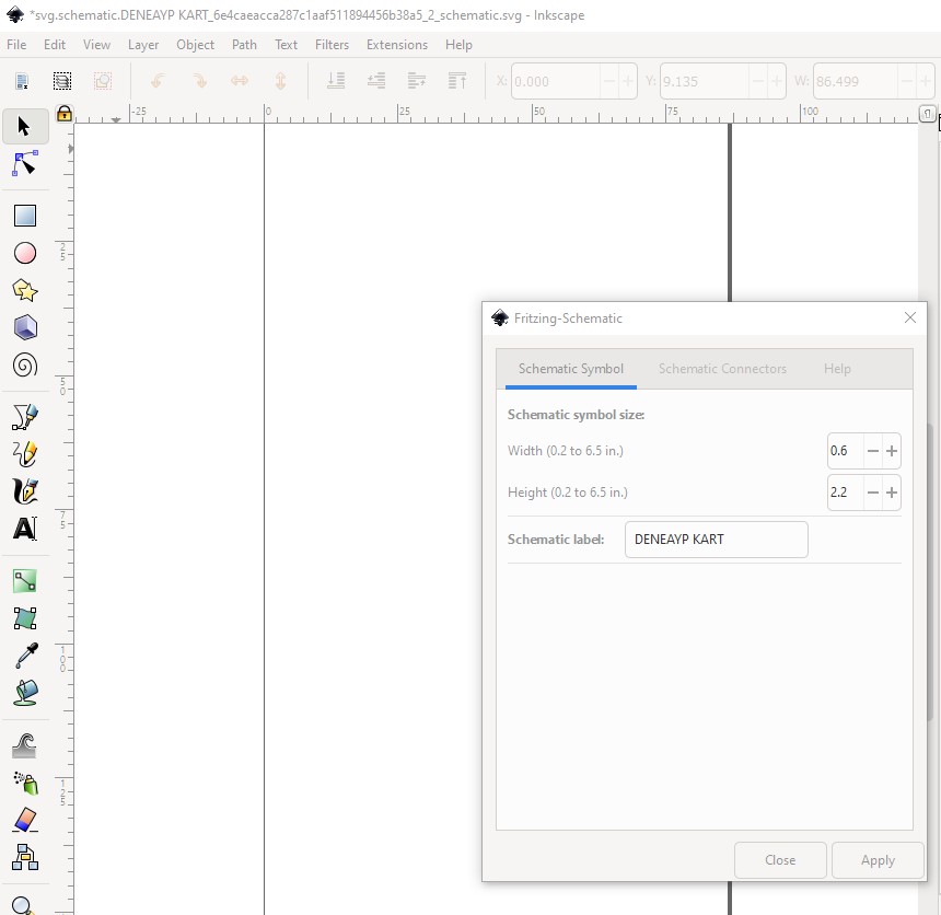
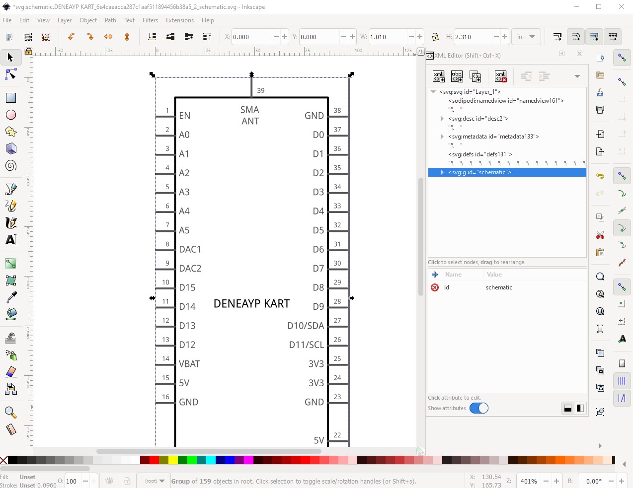
On to the schematic svg. The easiest way now to make this schematic is to use this Inkscape extension:
It will create a schematic svg with the correct pins, pin sizes colors and scale from an input template like this:
first we need to input the title for the part DENEAYP KART in this case then the width and height (which may be adjusted depending on the settings of the pins on the next screen!) In this case I set height to 2.2in (for 20 0.1 in connectors on the right side and 18 0.1in connectors on the left side) and 0.6in wide like this:
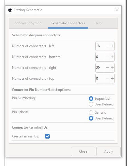
then switch to the Schematic connections tab and set the number of pins for each side like this:
clicking apply in the box brings up the labels screen. Now I need to add pin labels for the pins starting at connector0pin (from breadboard in this case) like this:
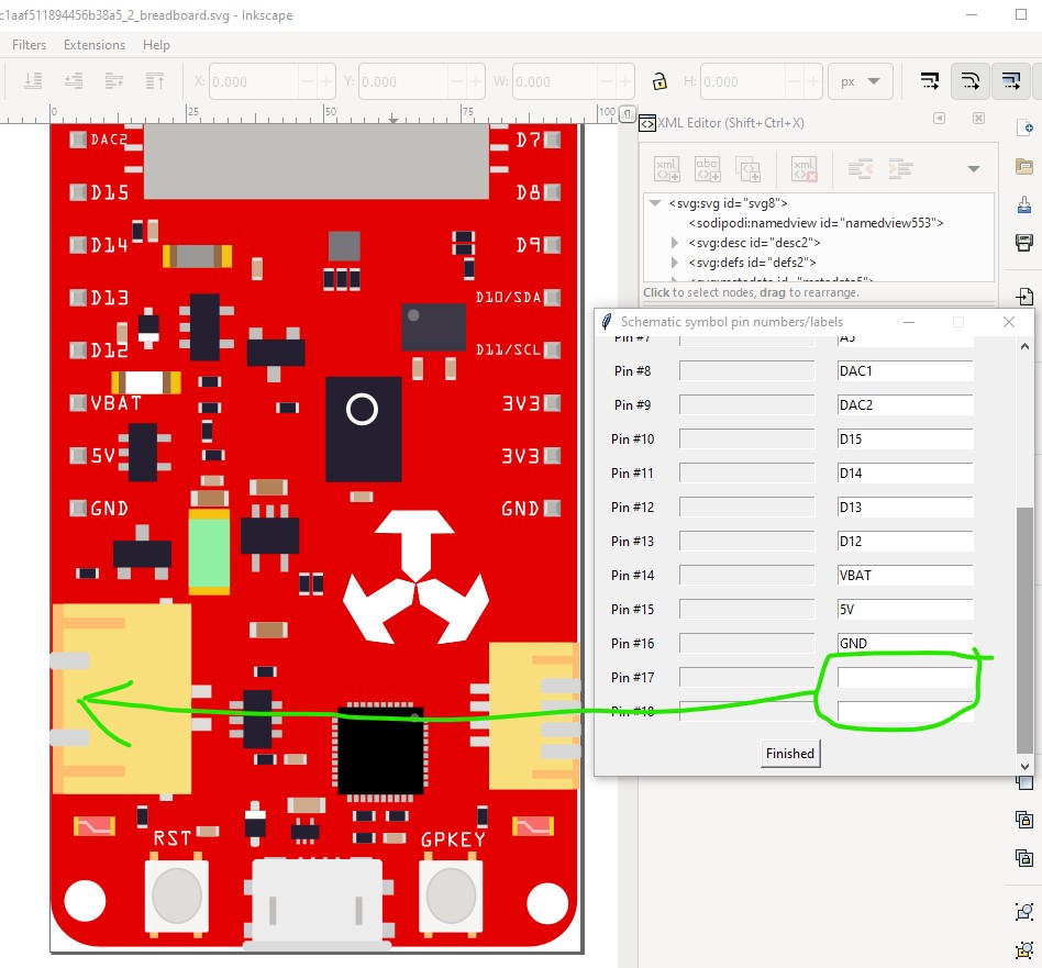
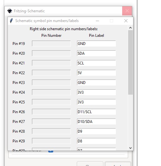
for the last two (which are not in breadboard) I needed to load the part in to Fritzing and grab the pin labels (BATTERY+ and BATTERY-) from there. Then I clicked Finished and it goes on to the right side pins (starting at the bottom of the screen which I also needed to get from the part in Fritzing as they aren’t labelled in breadboard and it ends like this:

at which point I click finished to create the schematic svg like this. Then close the Fritzing extension because we are done with it.
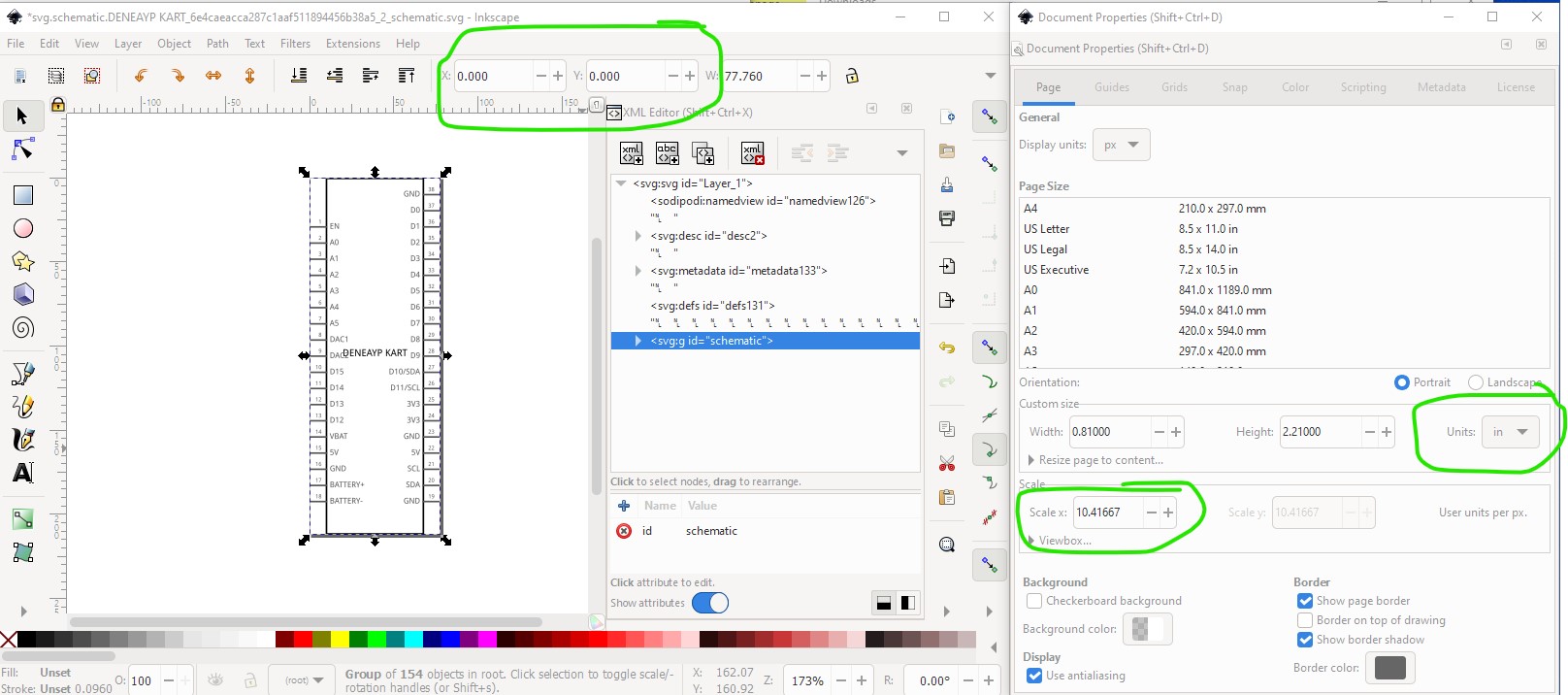
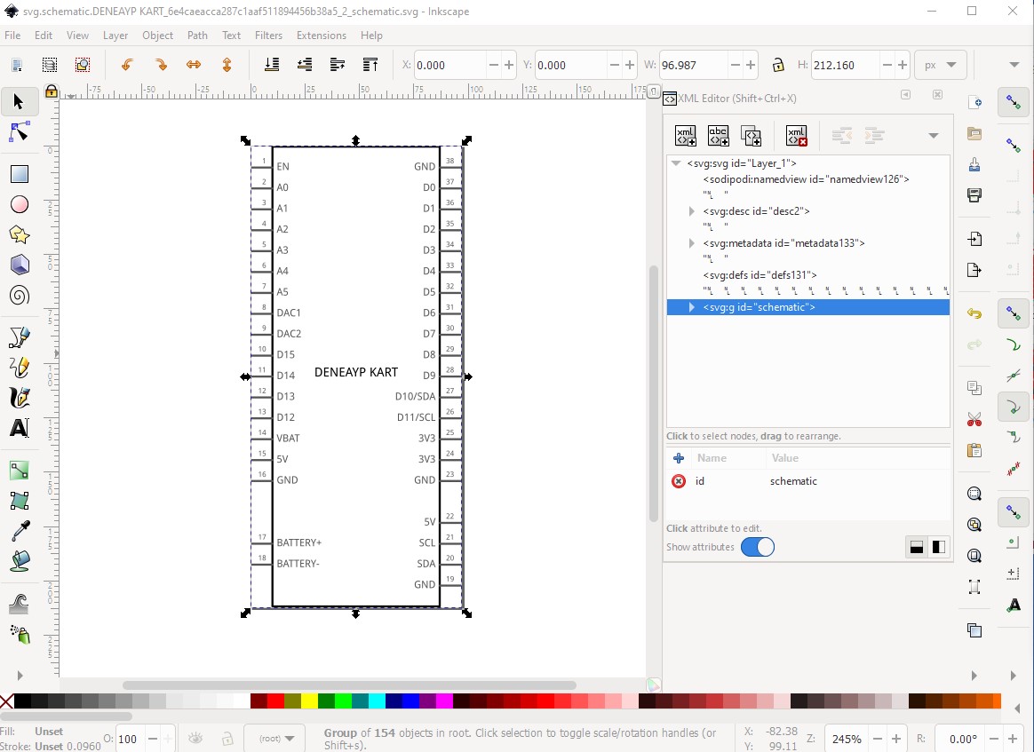
Here we see (circled in green) that the origin is 0 0 as it should be, the scale is 10.41667 as it should be and the units are in in as they should be. It turns out I screwed something up (too small in width) and need to move some of the connectors to their correct positions, so ungroup schematic and make the changes. First set the units to in so movement is easy (one click on the tool bar moves 0.1in!) and increase the width to 0.8in from 0.6in then move the DENEAYP KART label 0.1 higher in x to center it. Move the bottom 4 connectors on the right down 0.1in in y so they form an appropriately separated 4 pin connector. Move the first 16pins on the right up 0.2in in y so they match the right side 16 pins as they do in breadboard and schematic is finished. So Edit->Select all, Edit->Resize page to selection, Object->group and name the group schematic then save as plain svg and schematic is finished.
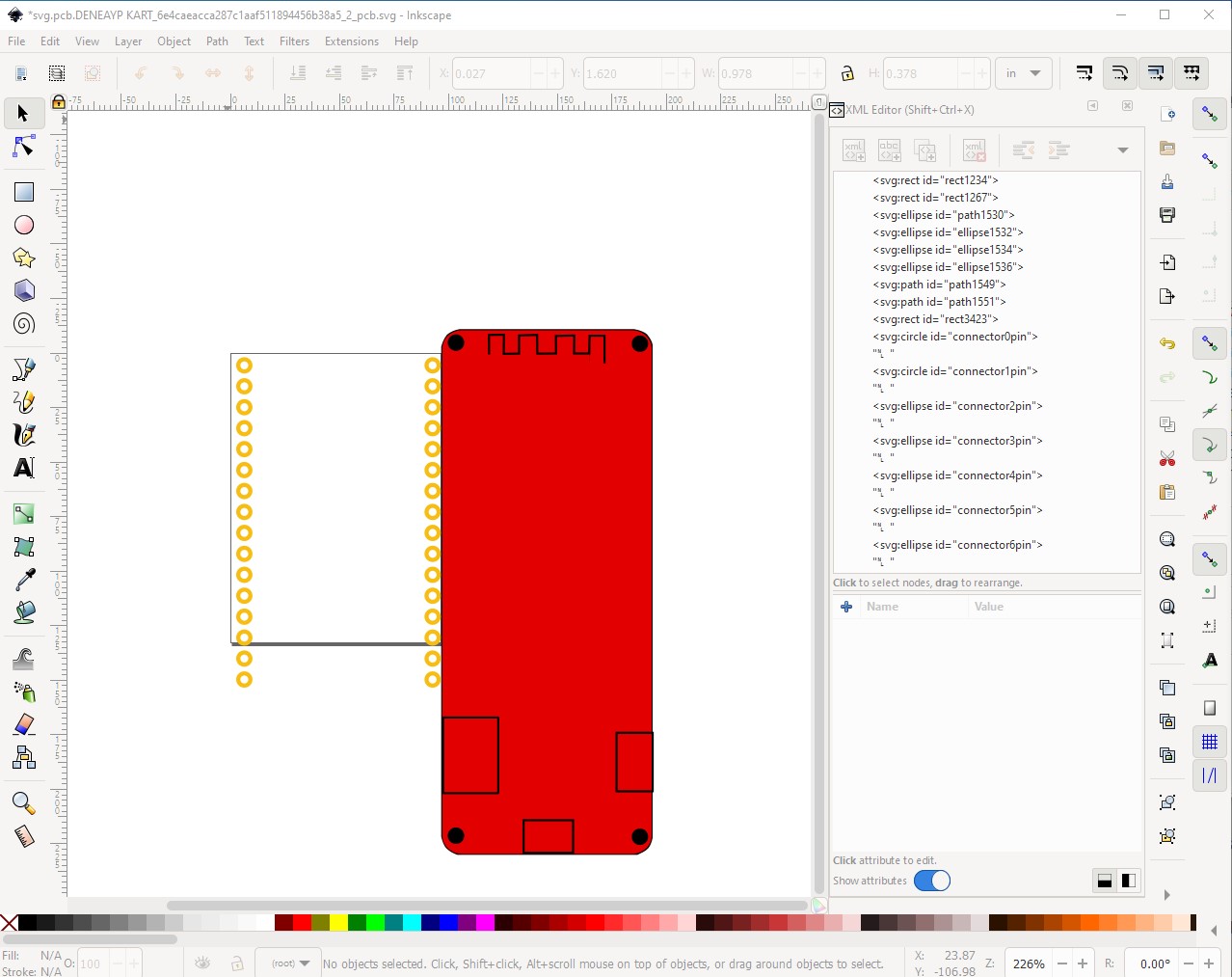
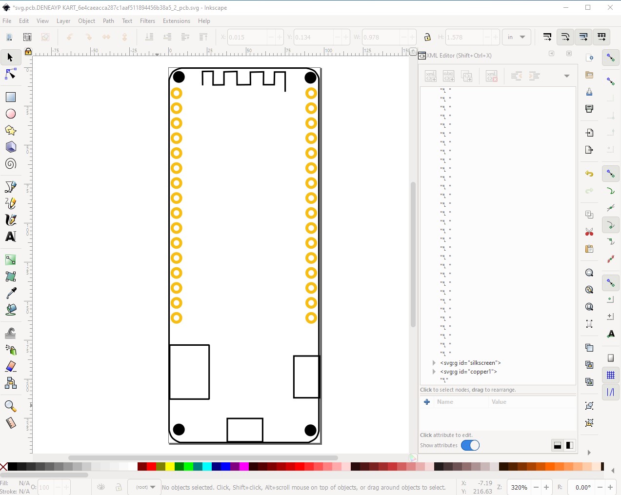
Now on to pcb. The current svg is dimensioned in px and thus scaled wrong. So rotate 90 degrees to match the layout of breadboard. Delete the silkscreen group (it is entirely wrong and unneeded.) Ungroup the copper groups. Edit->select all, Edit->resize page to selection, then rescale from 1.0 to 10.41667 the same as we did for breadboard. At this point I discover that the pads are paths (rather than circles.) While paths will work they are undesirable because a circle is much easier to set the hole size in. So set up an appropriate pad and call it connector0pin which produces this:
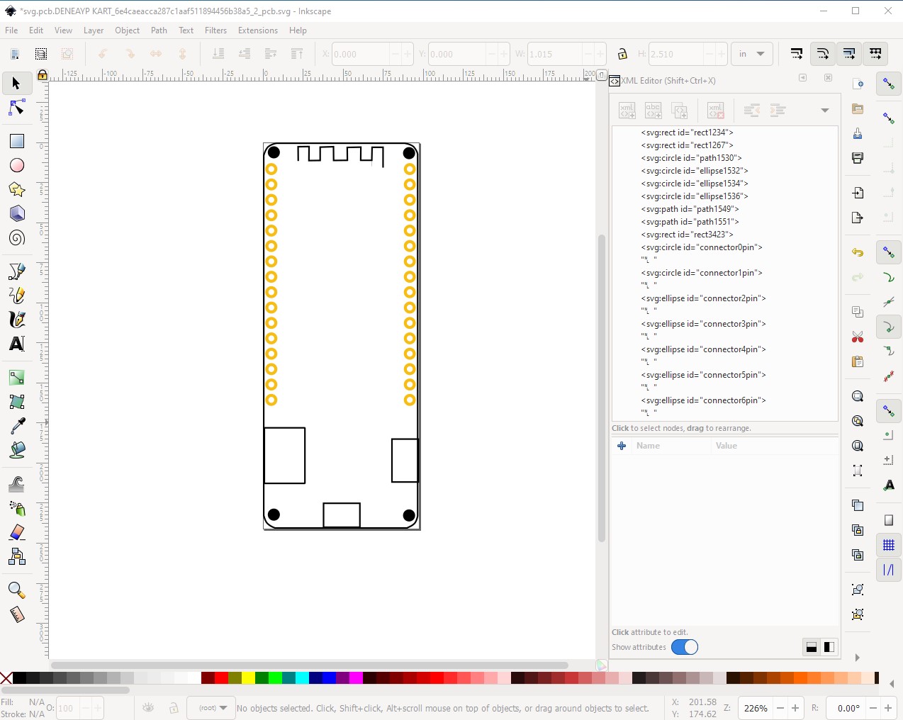
Here the scale is the correct 10.41667, the Units are in (not px!) so the scale will remain correct. The pad has a radius of 29 which corresponds to a diameter of 0.078in and the stroke-width is 20 (which will give a 20 thousandth of an inch ring to the pad. In Inkscape the diameter of the hole in pcb is calculated as
hole size = pad diameter - (2 * stroke-width)
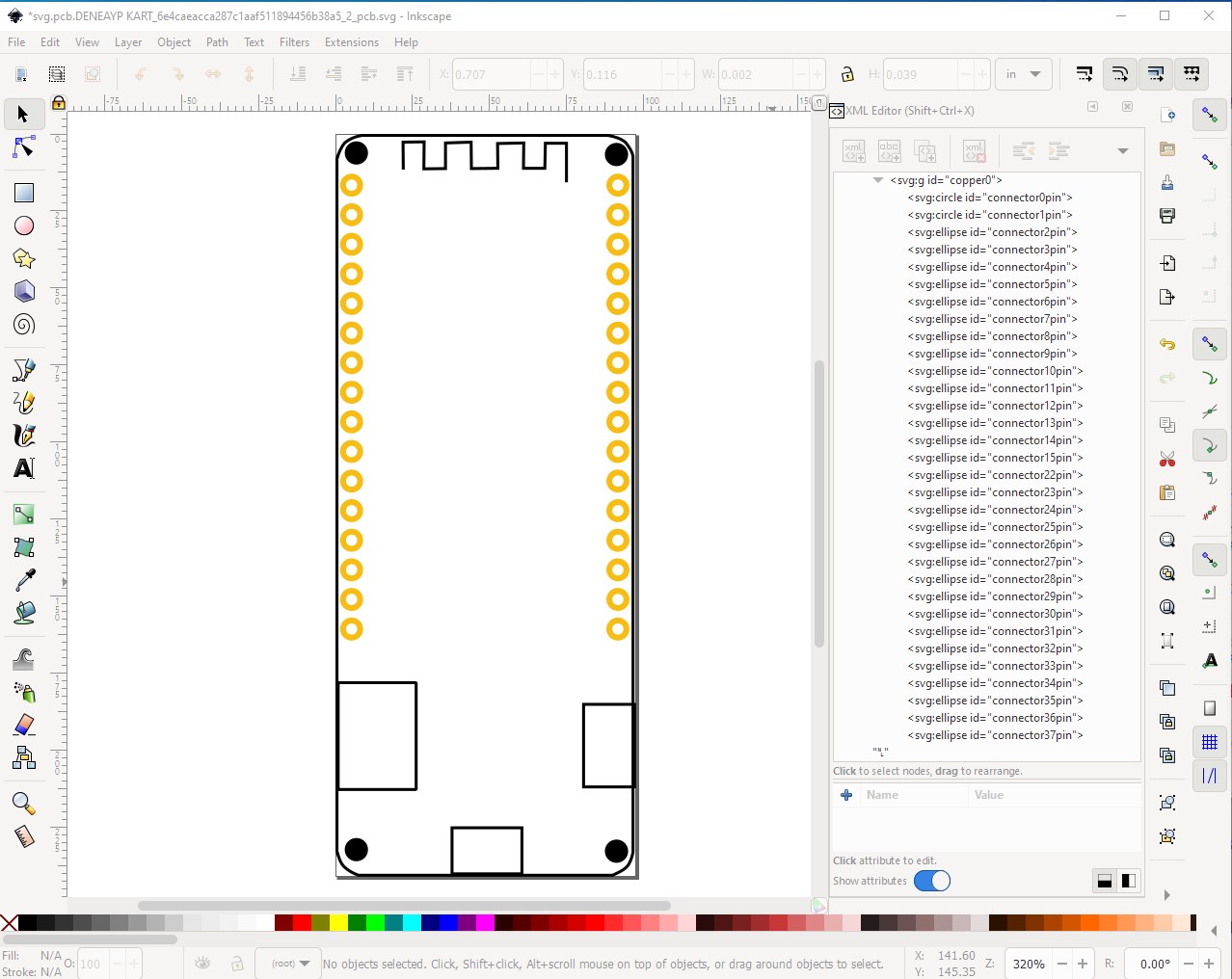
in this case the works out to a hole diameter of 0.038in which is the correct size for a 0.1in header connector (this diameter is 0.078in and the stroke-width is .02in.) Now we duplicate the existing pad and move it down 0.1in in y to create connector1pin, then repeat until we have all the same pins as in breadboard (we will eventually delete the 6 pins belonging to the battery and 4 pin connectors which don’t appear in pcb view but not until we have created the correct pin numbers!) At the 18th pin as well as adding 0.2in in y (to create the last 2 pins of the 4 pin connector on the other side) we also add 0.9in to the x coord to move the pin to the right side of the board in the correct place. Then I did
$ SvgSetConnectorsbb.py ‘svg.pcb.DENEAYP KART_6e4caeacca287c1aaf511894456b38a5_2_pcb.svg’
*** Process svg.pcb.DENEAYP KART_6e4caeacca287c1aaf511894456b38a5_2_pcb.svg ***
to again renumber the pins to create this svg:
which has the pins numbered the same as pcb (connector38pin which is the sma connector for the antenna also doesn’t appear in pcb and thus isn’t here.) Now I will delete the bottom 6 connectors which belong to the external connectors in breadboard and thus won’t appear in pcb like this:

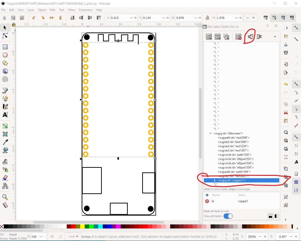
which after the delete looks like this with only the 2 groups of 16 connectors that are the 0.1in header connectors in pcb.
Here we see that connectors connector16pin to connector21pin are missing as they are in the connectors that don’t connect in pcb, but the header connectors do exist and match (which they must!) the pin numbers in breadboard. Now we need to build the silkscreen layer. To do that I will copy in the breadboard svg like this:
Here I have aligned the pads from breadboard to be in the center of the pads I just created in pcb. Now I will move the breadboard group 1in in x so it is beside the pcb pads (because I need to delete most of breadboard and then move the remainder back to its previous position by again moving it -1in in x!) Now I ungroup group breadboard and delete most of it except the parts (the base board, the mounting holes and the two external connectors) I want to be in silkscreen like this:
Note I couldn’t figure out how to convert the red rectangle to a path successfully (it shrinks probably due to stroke-width) so I created a new path and adjusted it to match the red rectangle which I then deleted to leave this:
which is the final (if yet ungrouped!) pcb svg. The Silkscreen shows the locations where the connectors need clearance for the wires that connect to them, the antenna (which presumably is a keepout area!) and the place where the mounting holes will go if you want mounting holes. All that is left is to group the pads in to copper1/copper0 and the silkscreen in to silkscreen like this:
and then do the silkscreen (by Edit->select All, group and unindenting the copper1 group which will be in the silkscreen group) like this:
to end up with the final pcb svg which looks like this:
and pcb is finished. Now we need to fix up the .fzp file to reflect the changes made in the svgs and the new pin numbering. Since the pins were out of order in the fzp file I chose to delete and replace the entire connector definition as being easiest.
  </iconView>
 </views>
 <connectors>

 </connectors>
 <buses>
  <bus id="SCLK"/>
  <bus id="GND"/>
  <bus id="internal1">
   <nodeMember connectorId="connector16"/>
   <nodeMember connectorId="connector13"/>
  </bus>
  <bus id="internal2"/>
 </buses>
 <url>https://deneyapkart.org/magaza/urun-deneyap-kart.html</url>
</module>
I then ran
$ FritzingCreateFzpConnectors.py t 39
(FritzingCreateFzpConnectors.py is available on github) to create a new set of connectors to add to the fzp like this:
  <connector id="connector0" type="male" name="">
    <description></description>
    <views>
      <breadboardView>
        <p svgId="connector0pin" layer="breadboard"/>
      </breadboardView>
      <schematicView>
        <p svgId="connector0pin" layer="schematic" terminalId="connector0terminal"/>
      </schematicView>
      <pcbView>
        <p svgId="connector0pin" layer="copper0"/>
        <p svgId="connector0pin" layer="copper1"/>
      </pcbView>
    </views>
  </connector>
  <connector id="connector1" type="male" name="">
    <description></description>
    <views>
copy this in to the .fzp file and then add the name and description fields (from breadboard or schematic) and you are mostly done (some of the connectors need to be modified to not appear in pcb!) At pin connector16 we need to delete the pcb definitions (for this pin and the next 6 to cover both connectors) like this:
 <connector id="connector16" type="male" name="BATTERY+">
    <description>BATTERY+</description>
    <views>
      <breadboardView>
        <p svgId="connector16pin" layer="breadboard"/>
      </breadboardView>
      <schematicView>
        <p svgId="connector16pin" layer="schematic" terminalId="connector16terminal"/>
      </schematicView>
      <pcbView>
        <p svgId="connector16pin" layer="copper0"/>
        <p svgId="connector16pin" layer="copper1"/>
      </pcbView>
needs to change to this:
 <connector id="connector16" type="male" name="BATTERY+">
    <description>BATTERY+</description>
    <views>
      <breadboardView>
        <p svgId="connector16pin" layer="breadboard"/>
      </breadboardView>
      <schematicView>
        <p svgId="connector16pin" layer="schematic" terminalId="connector16terminal"/>
      </schematicView>
      <pcbView>
      </pcbView>
at connector22 we start leaving the pcb definitions in again as they exist in the pcb svg. Connector38 (the sma antenna) also needs its pcb definitions deleted because it is not present in the pcb svg. As well I noticed at this point that connector38 is not shown in schematic and it needs to be there. So add connector38 to the top of schematic like this:
Now we need to fix up the buses. It looks like buses are needed for VBAT and BATTERY+ (I assume that VBAT is connected to BATTERY+ ? If not, then remove that bus from the fzp file!) BATTERY- should be part of the ground bus. The 5V pins, 3V3 pins SDA and SCL all appear to need to be in buses (I am assuming they are connected together internally! If that is not true then again, remove the affected bus definitions in the fzp file.)
So the GND bus needs to include pins
connector15 (GND)
connector17 (BATTERY-)
connector18 (GND on I2C connector)
connector22 (GND)
connector37 (GND)
The 5V bus needs
connector14 (5V)
connector21 (5V on I2C connector)
The 3V3 bus needs
connector23 (3V3)
connector24 (3V3)
The SDA bus needs
connector19 (SDA on I2C connector)
connector26 (D10/SDA
The SCL bus needs
connector 20 (SCL on I2C connector)
connector 25 (D11/SCL)
again I am assuming the SCL and SDA pins are shared, if they are not then the bus definition needs to be deleted. That should complete the fzp file and the entire part. So now we run it through FritzingCheckPart.py to make sure we didn’t make any mistakes then make the part and test it in Fritzing like this:
 <bus id="GND">
   <nodeMember connectorId="connector15"/>
   <nodeMember connectorId="connector17"/>
   <nodeMember connectorId="connector18"/>
   <nodeMember connectorId="connector22"/>
   <nodeMember connectorId="connector37"/>
  </bus>
  <bus id="5V">
   <nodeMember connectorId="connector14"/>
   <nodeMember connectorId="connector21"/>
  </bus>
  <bus id="3V3">
   <nodeMember connectorId="connector23"/>
   <nodeMember connectorId="connector24"/>
  </bus>
  <bus id="SDA">
   <nodeMember connectorId="connector19"/>
   <nodeMember connectorId="connector26"/>
  </bus>
  <bus id="SCL">
   <nodeMember connectorId="connector20"/>
   <nodeMember connectorId="connector25"/>
  </bus>
which should implement all of those buses. Now run the whole thing through FritzingCheckPart.py to see what I missed. The only serious complaint is Inkscape’s fault, it has not translated the ellipses with the same radius in rx and ry in to circles (with a single r value.) This breaks gerber processing (it doesn’t generate holes for the pads that are an ellipse.)
Error 65: File
‘svg.pcb.DENEAYP KART_6e4caeacca287c1aaf511894456b38a5_2_pcb.svg.bak’
At line 210
Connector connector2pin is an ellipse not a circle, (gerber generation will break.)
Error 74: File
‘svg.pcb.DENEAYP KART_6e4caeacca287c1aaf511894456b38a5_2_pcb.svg.bak’
At line 210
Connector connector2pin has no radius no hole will be generated
There are several ways to fix this (all of them painful.) I’m first trying the latest version of Inkscape to see if the bug has been fixed. If that doesn’t work I’ll try the other workarounds (editing the file with a text editor, or getting Inkscape to correct the radius which sometimes happens but I’m not sure what needs to be done to cause it.) It looks like checkpart didn’t find any other errors other than pcb pads that are ellipses. Lets see if the new Inkscape release will fix this. It may have done some but the others are a floating point roundoff error (rx and ry here should both be 29, not rx 28.999962!) so correcting this with a text editor should be the quickest way to fix this.
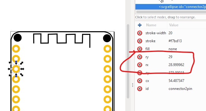
Ah! It appears moving the pad .1 in left then back right corrects rx and ry to an r so do that for all the pins (see if a mass move will do it!) Indeed it did, FritzingCheckPart now passes without error, so on to testing the new part in Fritzing. First problem, connect the board to breadboard to see that it connects correctly then check the various bus connections (which all look fine.) The problem is that SCL is shorted to the SDA pin on the 2mm connector.
The fix for that is to change the type field all 6 connector connectors from male (will mate with the breadboard) to female (which will not mate with the breadboard.) So do that and restart the testing. So in the fzp file change this:
<connector id="connector16" type="male" name="BATTERY+">
  <description>BATTERY+</description>
  <views>
to this for the 6 pins on the external connectors (connector16-21)
<connector id="connector16" type="female" name="BATTERY+">
  <description>BATTERY+</description>
  <views>
Then run checkpart and test the part again. This adds this warning to the FritzingCheckPart output:
Warning 11: File
‘part.DENEAYP KART_63dd7a12b8c4a450c43bd296078a8194_12.fzp.bak’
At line 310
Type female is not male (it usually should be)
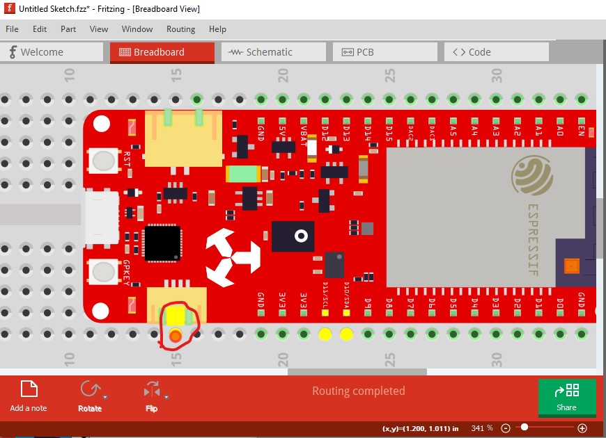
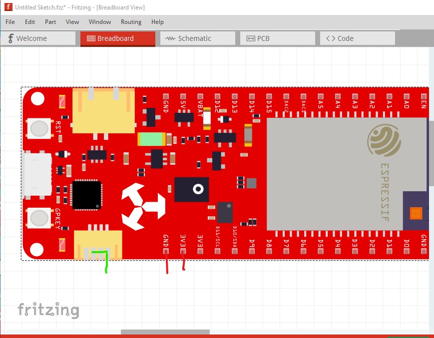
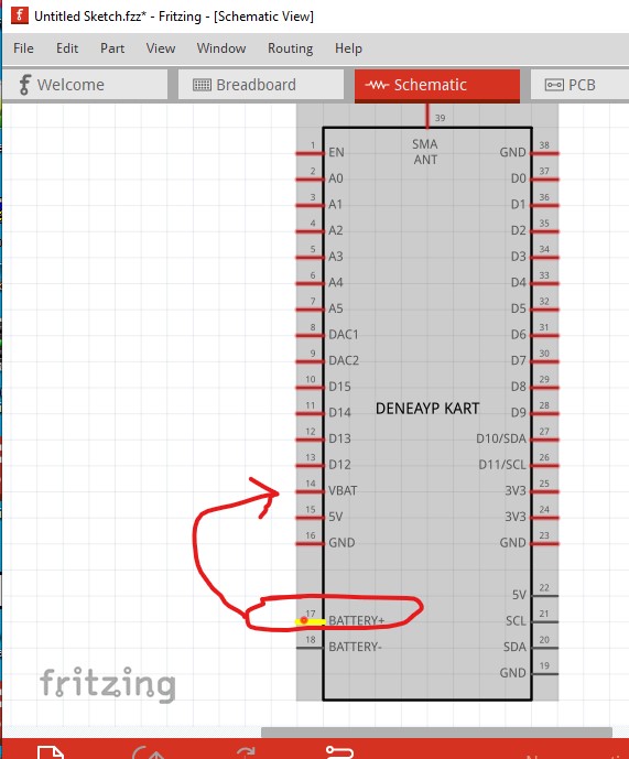
but otherwise all is fine and this is what we intended to do so proceed to test the part again. This promptly causes a new problem. Fritzing has chosen to align a pin of the 2mm I2C connector (the two green lines in this image) to the grid. That makes the rest of the pins (the red lines on GND and 5V a couple of pins up) not align to the grid.
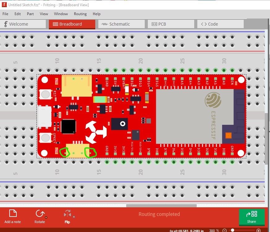
The only solution to this that I know of is to cause the pins in the 2mm connector to be on the .1in grid (so all active pins are on the .1in grid!) Otherwise this part may sometimes work (when a connector on the grid is selected as the anchor) and sometimes be like this when one of the 2mm connectors is selected as the anchor. Back around the loop yet again, modifying the breadboard svg this time. The solution is ugly, but the only one that I can see that will work. I duplicated connector22 pin them moved it down in y on .1 intervals and dupped 3 more of them for the 2mm pins. I then moved the 2mm connector out of its correct position to be centered on the new 4 pins. This will insure the pins are always on the .1 grid at the expense of making the 2mm connector not quite correct in breadboard (its position will be still correct in pcb silkscreen though because I don’t need to move that!) Doing the same to the battery connector on the other side should fix this.
So back through the loop yet again with the new breadboard svg and see what happens.
Indeed this time it works and all the pins align correctly even if the ones on the 2mm connector are not withing the connector body. As far as I know this is as good as we can do! Switching to schematic I promptly find another error: the label field in the fzp file should be set to M (for module) so this becomes
M1
DENEYAP KART
rather than:
DENEYAP1
DENEYAP
Moving to schematic and checking the buses turns up another error:
the BATTERY+ connector should be bused to VBAT but it is not (as VBAT has not lit yellow when BATTERY+ is selected.) so fix that as well. While I’m here I switched to pcb view and exported the part as a gerber to make sure gerber processing ran correctly. Viewing the results in the gerbv gerber viewer indicates all is well:
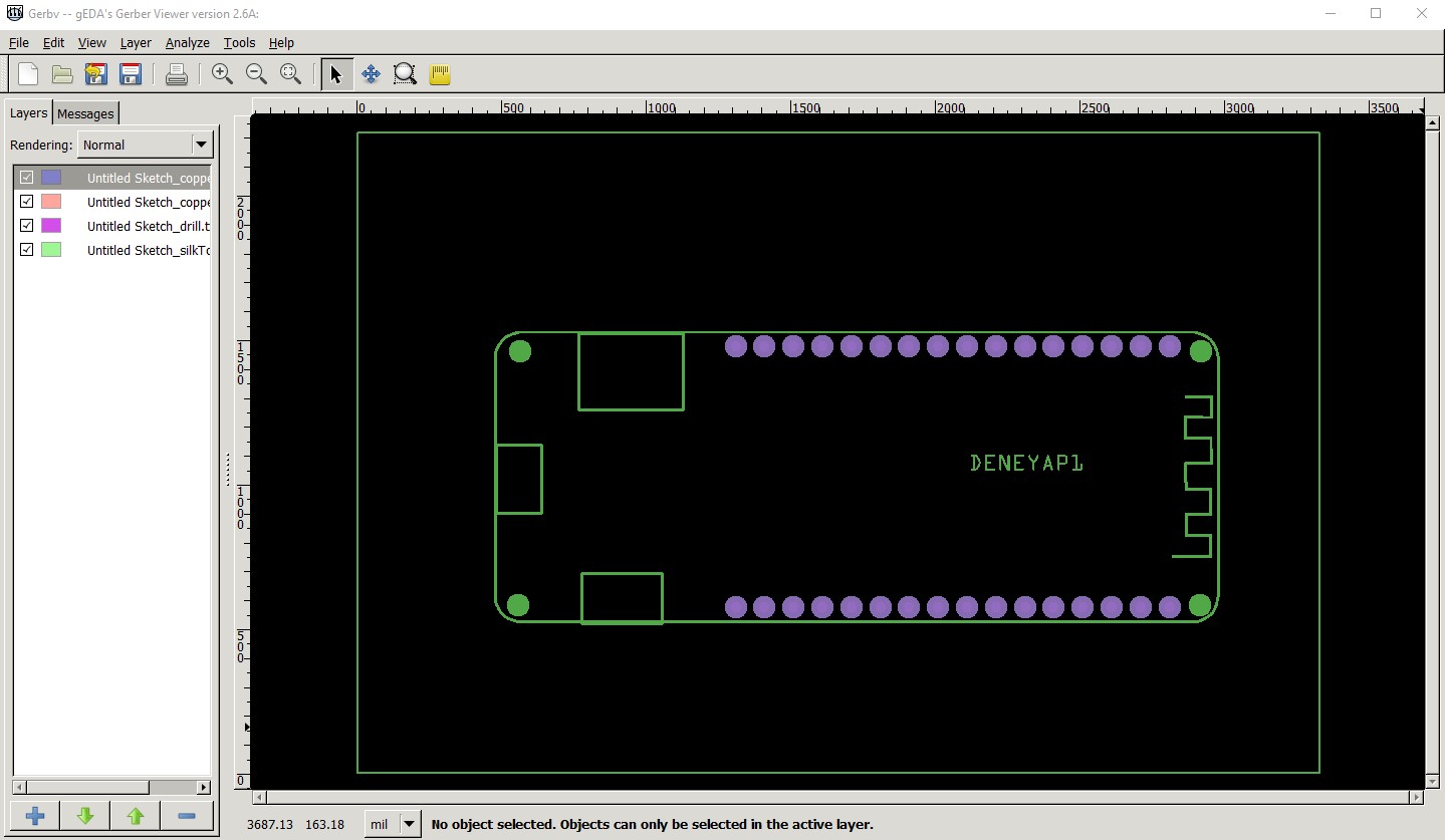
suppress copperbottom and coppertop layers to leave only the drill layer and check all the expected holes have been drilled.
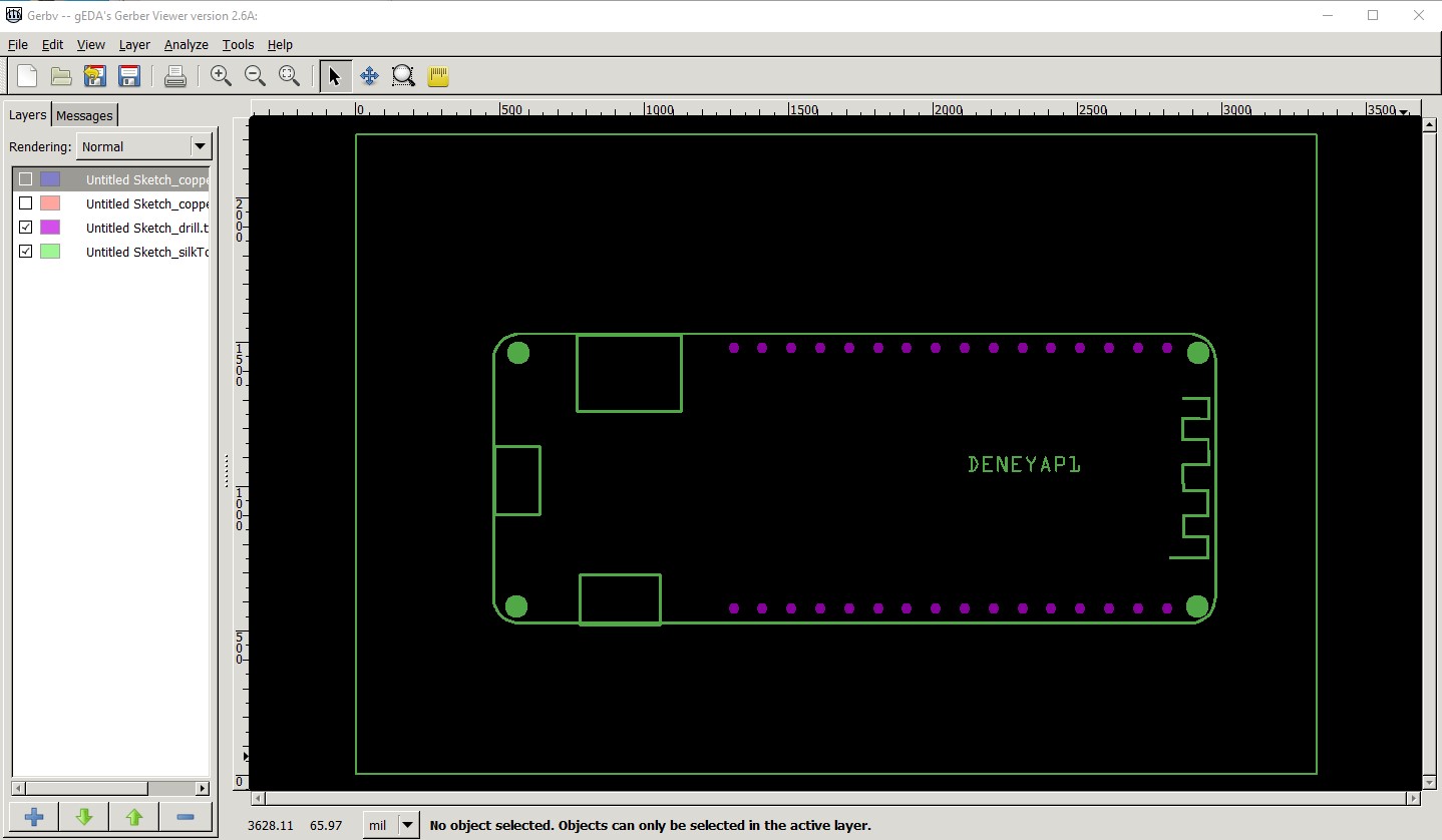
Check the drill.txt file to make sure they are all 0.038in:
; NON-PLATED HOLES START AT T1
; THROUGH (PLATED) HOLES START AT T100
M48
INCH
T100C0.038000
%
T100
X027111Y014777
X023111Y005777
…
M
which they are so all is well. Make the corrections noted above and try again. In the fzp file change label to M and add KART to the part number like this:
<label>M</label>

<property name="part number">DENEYAP KART</property>
Then add a bus for VBAT which I completely missed above and we should be done.
  <bus id="SCL">
    <nodeMember connectorId="connector20"/>
    <nodeMember connectorId="connector25"/>
  </bus>

  <bus id="VBAT">
   <nodeMember connectorId="connector13"/>
   <nodeMember connectorId="connector16"/>
  </bus>
</buses>
Through the loop yet again and back to testing. At this point all looks good. Here is the test sketch that checks everything:
DENEYAP-KART-test.fzz (45.6 KB)
and the fixed part (which is also in the temp parts bin in the sketch!)
DENEYAP KART-fixed.fzpz (28.9 KB)
This should be ready to submit via a pull request on github for inclusion in core parts. Hope this helps!
Peter