Hy everyone!!
Does anyone have a Fritzing version of this part?
Thanks!
There doesn’t appear to be one, but I have a single Fet version I made for someone a few years ago and it is relatively easy to modify in to this which should do what you want. PCB may be somewhat inaccurate because it was created from a scaled jpeg image of the board because there is no mechanical drawing I can find. Assuming you have one of these (which seem likely given you wanted the part  ) if you print out the footprint at 1:1 scale and feed back corrections on connector and mounting hole spacing I’ll correct it. As well the mounting holes are only on silkscreen as usual. If you want mounting holes you need to drag a hole from core parts pcb in to the sketch over the mounting hole on silkscreen.
xy-mos-d4184.fzpz (11.5 KB)
Peter
Thank you, will work great.
I’ll check if corrections are needed.

Hy everyone!!
Does anyone have a Fritzing version of this part?
[https://www.kuongshun-ks.com/uno/uno-board-shield/mosfet-electronic-switch-dc-controlling-broad.html]
Thanks!
thanks you <3 i am vietnames
You came through again. Thank you very much!
Hey there, sorry to dredge up an old thread but I have a relevant request.
Thank you SO MUCH Vanepp for making this part! It’s almost what I need :-\
I need one that’s a little more detailed, with oversize holes in the PCB for the legs of the terminal blocks to solder in place, as though I was going to mount the terminial blocks or solder in an 18GA wire.
I’ve designed a board that uses these little pwm modules as daughterboards, they piggyback on it and the legs of the terminal block stick down through a 1.5mm via/through hole where I can solder them in place ![]()
I understand enough to know that modifying this part should be trivial, alas, I have never been able to wrap my head around the process for making Fritzing parts from scratch so I’m stuck.
Vanepp, if you, or someone else could take pity on me and tweak this part with those holes I’d be very gratefull.
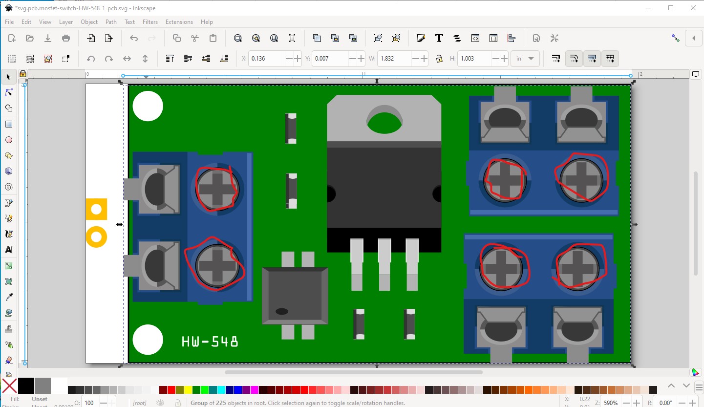
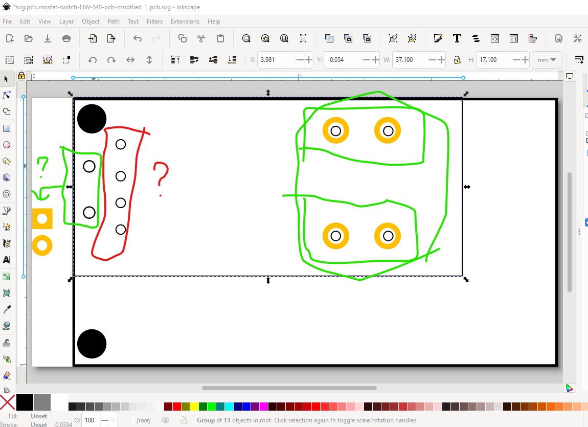
Easy enough to do, but I need more information. Presumably you want holes (1.5mm diameter) in pcb where the terminal blocks are
presumably near the red circles. I need the x/y coords of each circle’s center point From the top left corner of the pcb to position the holes. In or mm either if fine for positioning. (the holes for the real terminal block may however not be where they are depicted here, as I recall they are closer to the center of the outside block!)
Peter
Oh wow, thx. Here’s the specs.
First hole, top terminal block, 25mm from left edge of board, second, 30mm. Both are 3mm from the top edge of the board.
The bottom holes, same horizontal distance, 13mm from top edge of board.
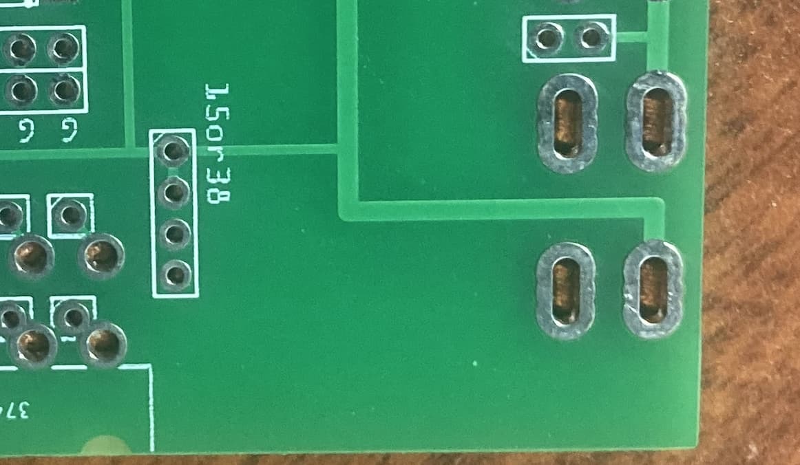
edit: Here’s a pic of the spacing on my board.
edit2: The spacing of the four small/two larger holes for the driver signals are already in the correct positions.
I think I am misunderstanding something (and images upload here just fine, this is a jpeg image, upload is 7th icon from the left in the reply menu!)
I’d expect the new holes to more closely match the position of the screw terminals in breadboard (which indicates I may be missing something!) The new holes are 3mm below the top of the board and 25mm and 30mm from the left edge of the board. I think what you are trying to do is extend the pins of the two left terminal blocks in to a pcb under the module (but I may have misunderstood!)
Peter
Yes, I’m extending the two pwm signal pins on the left down through another pcb. The whole spacing for the two larger holes and the 4 standard size holes in the part is correct.
I also want to let the 4 terminal block pins, which already stick through the pwm pcb by an exta 2 or 3 mm, to extend through elongated holes in my board design so I can just pool some solder on them to solder the pwm board down.
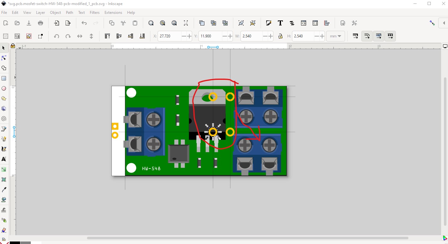
The 4 holes on the right end need to be a center to center 5wide 10 tall, with the center of the top hole 3 mm from the edge of the board and center of the bottom hole 13 mm from the top of the board. Pattern like so.
_________________________________ top edge
| |
| 3mm
| |
|_____________________25mm________O__5mm__O
| |
| 10mm
| |
|_____________________25mm_______O__5mm__O
|
|
|
________________________ bottom edge
The center of the top left hole should be 25mm from the left edge of the board.
These holes at the left end of the existing board design are fine
--------------------O-----O
----o
0_o
0_o
----o
--------------------O-----O
I need 4 regular size, or slightly larger holes, in aprox the positions the capital Os are in.
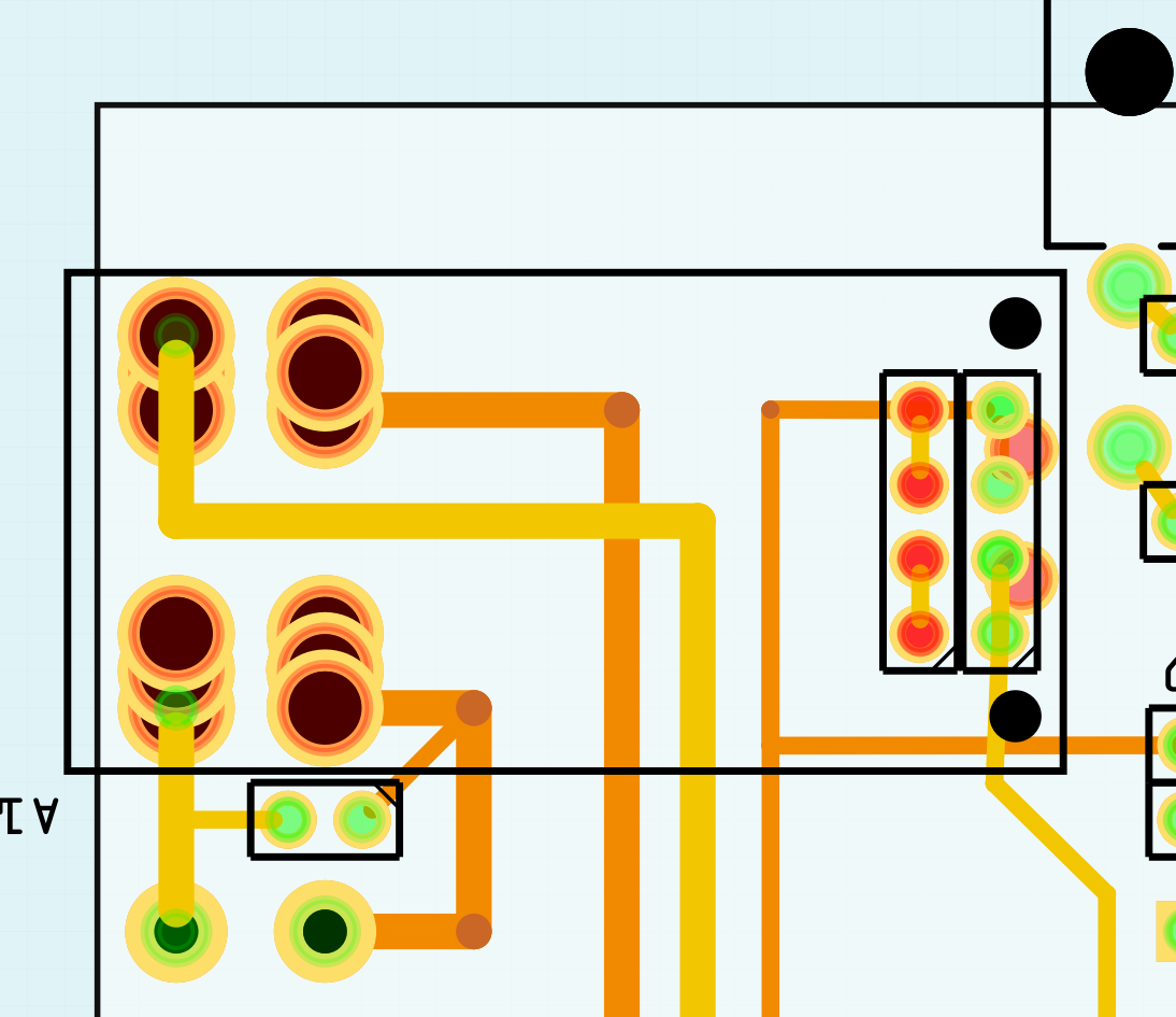
OK this part should do what you want.
mosfet-switch-HW-548-pcb-modified.fzpz (12.3 KB)
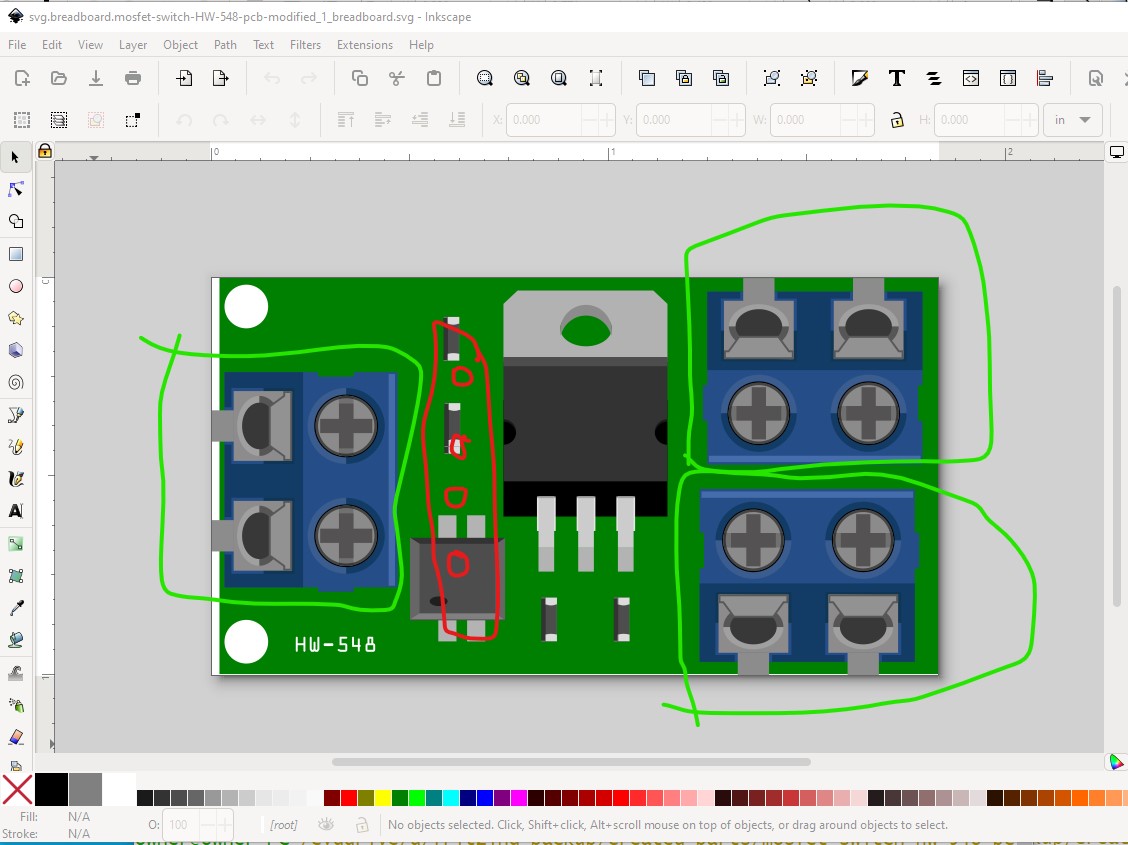
It produces a pcb like this
Where the 4 new holes are 1.5mm (0.060in) and connect to the two right most screw terminals.
Peter
OK, so assuming the svg is to scale, the pcb you have is smaller than the current part (which isn’t a problem) but I need to know what the additional holes connect to in breadboard and schematic
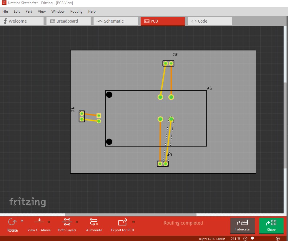
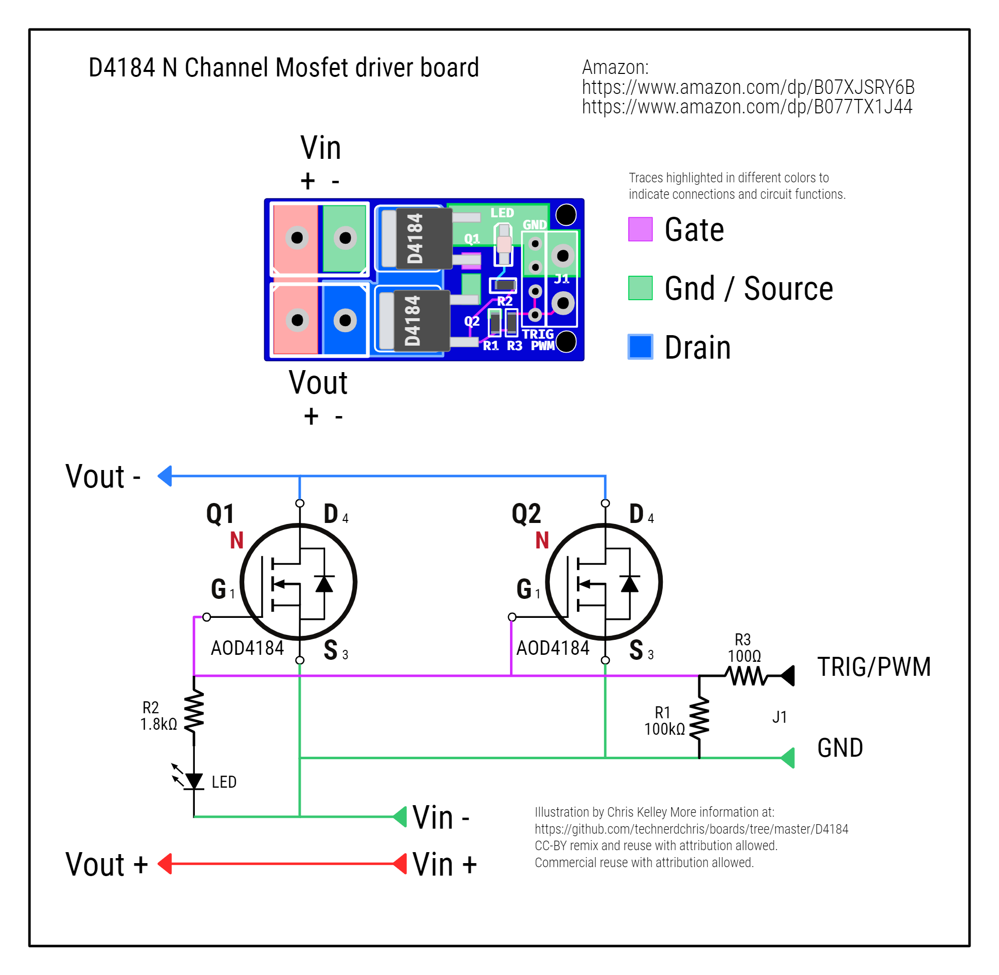
which corresponds to the current breadboard like this
The screw terminal on the left is the control input, what the other 4 holes correspond to isn’t clear and the right two screw terminals are the Output of the MOSFET (source and drain) with each pin of the top and bottom screw terminals connected to each other internally on board (and the source and drain of the MOSFET.) I need to know what the additional 4 terminals do to make a complete part. Actually the layout of the breadboard view of the part would help as well.
Peter
Now with fresh eyes and a steady caliper I’ve updated the svg to match the board, edited the prev post with it, and added a schematic of the module.
That makes things clearer. I’ll post an updated part in a while.
Peter
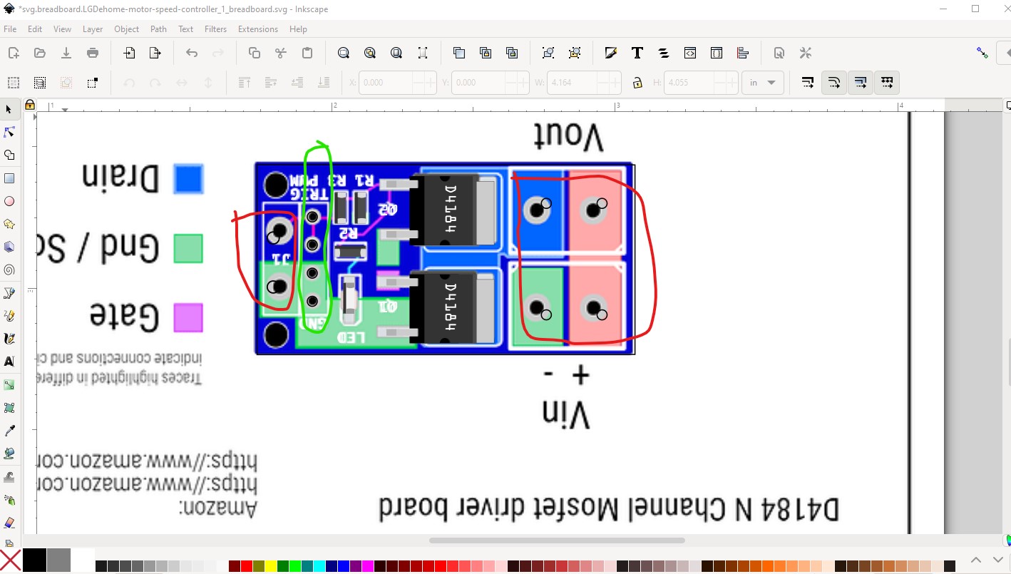
OK here are two new parts. The reason there are two is your svg doesn’t match the scaled jpg image and I don’t know which one is correct so I made both and you can use which ever best fits your needs.
This is the jpg image superimposed on your svg. As you see the 4 0.1header pins match, but the screw terminal pins are off a bit. The jpg positions would match 2mm pitch screw terminals (and I think is mostly likely the correct one!) Here are the two parts
LGDehome-motor-speed-controller-jpg.fzpz (7.7 KB)
LGDehome-motor-speed-controller-svg.fzpz (7.8 KB)
the one marked -svg has the pads that match your svg, the one marked jpg matches the jpg image layout. Printing out both footprints at 1:1 scale and comparing them to a real board should tell which one (if either!) is right.
Peter
The file named .svg matches actual spacing for the boards I have.
THANK YOU THANK YOU THANK YOU.
This will make it SO much easier to revise my aquarium controller board design as it evolves. These 4184 boards are so ubiquitous there’s bound to be other folks who will benefit from your part after google points them to this thread ![]()