Hello,
I have 2 “Wire overlapping” messages when I run DRC.
How could I avoid those errors ?
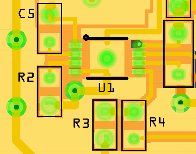
Here is a screenshot of the zone.
Problem is located on bottom pins of U1 (pins 4 & 5):
Here is my project file:
LM5007.fzz (47.6 KB)
Wali
Hello,
I have 2 “Wire overlapping” messages when I run DRC.
How could I avoid those errors ?
Here is a screenshot of the zone.
Problem is located on bottom pins of U1 (pins 4 & 5):
Here is my project file:
LM5007.fzz (47.6 KB)
Wali
I could not find anything wrong with it and I could find nothing wrong with the part… The pad spacing is less than 10mil apart. It looks to me like Fz is throwing a false error. Fritzing has a tendency to through errors when traces and pads are close together, we have ran across that when running traces between pins… we just ignore them. When I moved the chip just a little bit it through the errors on the other pads. I would say just go ahead with it… as far as the errors go, I can’t see a problem.
If you move location up to 0.635 or down to 0.639in it clears.
Don’t know if it matters but one pad is 1 px out.
It looks ok, but maybe gerber it to be sure.
Fritzing idiosyncrasies… 
Thank you for your responses.
As has said Old_Grey, I have moved part location down to 0.639, and there is no more errors.
But Steelgoose, you have said: [quote=“steelgoose, post:2, topic:1891”]
I would say just go ahead with it…
[/quote]
Does this means that if I send this file to fab with DRC errors like those, it will be accepted and produced, or have I to look for a solution like the one proposed by Old_Grey before sending the file for fab ?
I would say it is just a Fritzing thing  I doubt very seriously that there are any real errors… It is just the way Fritzing DRC scans it…
HI. I am using VIAS as connection points on my PCB which, in turn, have tracks connecting to them. I am getting a heap of “overlap” errors in DRC. Is this an actual concern… or will manufacturing from Gerbers effectively deal with this? If it is a problem how do I deal with it?
Thanks…
We would need to see the actual fzz sketch file to tell. It depends on the specific case whether it will be a problem or not.
You can also export the greber, then use a viewer with that to visually inspect to see if any of the errors are real.
The message could indicate an actual overlap, or traces (or pads) too close each other for the settings in DRC. Which is typically 10 mil.
How to deal with it also varies. Move the vias. Make the traces narrower. Reduce the pad size for the vias. Reduce the DRC clearance setting (staying within the limits that the board production house uses). Any of those might fix the reported problem. In cases of real overlap, you might have to reroute the board, perhaps rethinking the layout of the parts.