Hi
I’m a first-timer and I’m working on a project with a very short deadline. Could someone please cast their eyes over my project before having it fabricated? Willing to donate for time etc.
Very simple project but tbh I don’t really know what I’m doing with fritzing. It’s a teensy breakout board for a bunch of analog pins to a 36 pin connector. I know that what I want to build works(I’ve soldered one manually, just never tried a pcb) so I’m really just concerned with trace contrinuity and best practice.
I tried getting the ground to the gnd pins on the connector using them as ground fill seeds but have ended up using a bunch of vias in an ugly configuration. Will this thing wo
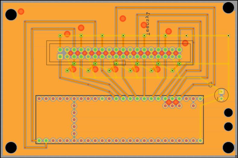
This should work (for some value of work). The routing is ugly and should really be simplified a bunch. There are no board limits either so it will be quite a bit larger than it should be as well. If you were intending to have copper fill, that is not present. If you click file->export for production->extended gerber that will create the gerber files that the board will be produced from. From there a gerber viewed such as gerbv will show you exactly what the copper will look like. As noted the posted fzz file has no copper fill in it and no mounting holes.
Edit: on a closer look, the teensy part has a number of errors which may be affecting your layout. I’m having a look at correcting the part.
Peter
Thanks, I just don’t know how to simplify the routing, any advice would be appreciated.
Bit of a worry about the teensy part, I found it somewhere or other and I think people had been over it a couple of times. So you mean it is the wrong size? How will it affect this layout?
Not so much the wrong size, as wrong size holes and internal troubles. Some of the internal connectors are male instead of female which means with it attached to the breadboard as you have it some of the pins will short (which may affect routing). I just discovered the internal pin numbering is a bit wrong as well. I’m almost finished fixing it up, once that’s done I’ll try and substitute it in to your sketch and see what (if anything) breaks. With a proper part in place I’ll have a look at routing. As noted the fzz that was posted doesn’t have the mounting holes (and so I don’t know where they should be on the pcb nor how large they should be).
Edit: as usual I’m wrong  , the current part is lacking some pin numbers which doesn’t matter to you for routing, but does for a proper part, so a new part isn’t going to do for you (because you would have to start the layout again from scratch). I’ll have a bash at a partial modification that should clear most of the immediate problems and have a look at your current layout and do a proper fix of the part later.
Peter
thanks again, i know the file changed before the screenshot. Teensy Breakout1.fzz (176.0 KB)
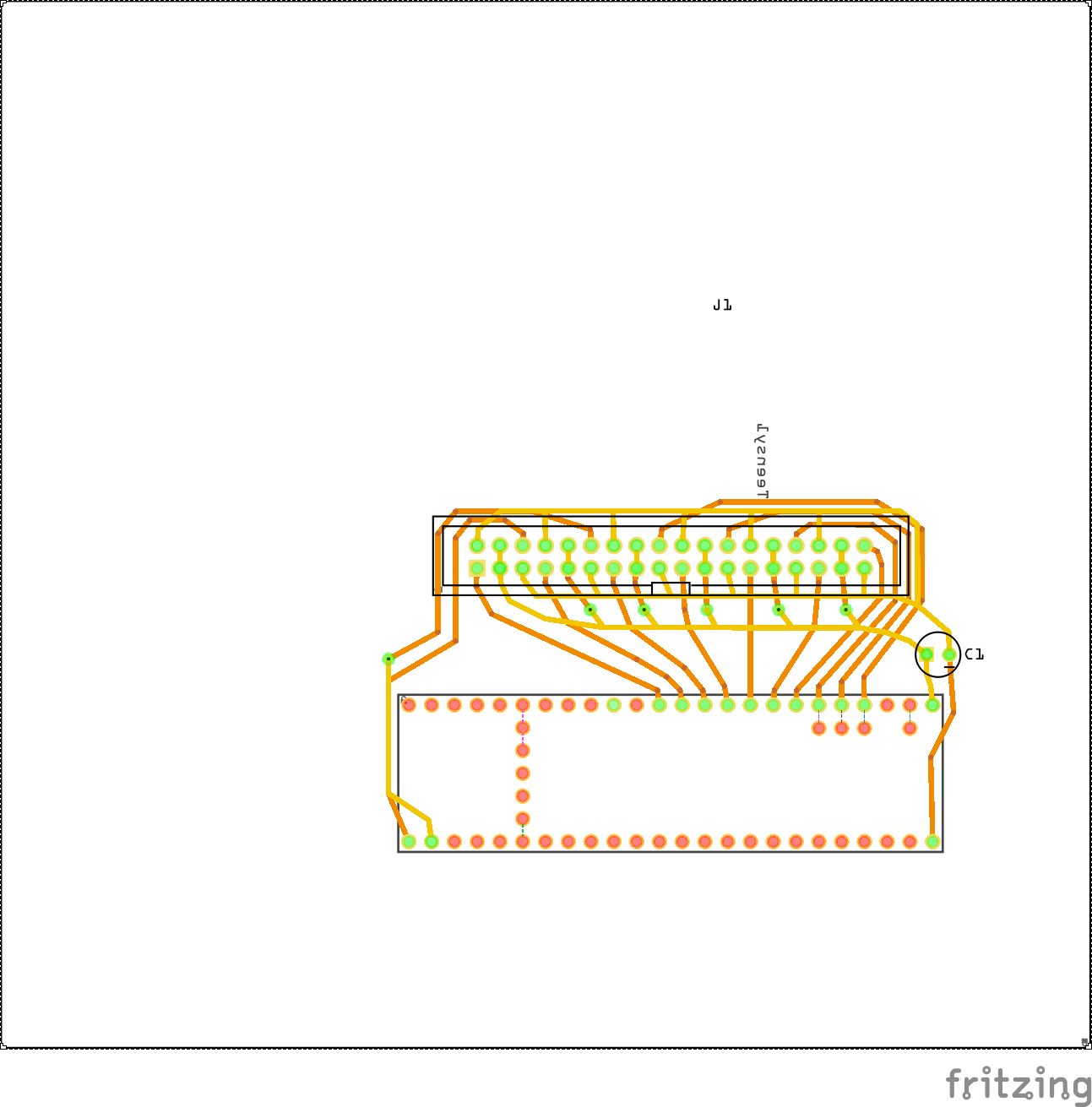
Perhaps you hadn’t saved it yet before export. In any case the new version is more complete than the original. As far as I can see it should work as is although the board appears to be inverted (i.e. looking up from the bottom) when it should usually be looking down from the top. This matters because the pins on the teensy will be in the wrong place if that is true (unless you intend on putting the teensy on the bottom of the board for some reason). Some of the hole sizes are a little large (.040 rather than .038 which is standard for .1 pins) but that shouldn’t matter that much. Is this intended to be home etched is that the purpose of all the ground fill? Here is what gerbv thinks the gerbers will produce from the current version:
Meanwhile I’ll have a poke at making a better routing layout although it will probably be without the ground fill.
Peter
The ground fill was just because I had read it to be a good practice, both for board rigidity and training any ambient interference. Not a good idea?
No I didn’t plan on mounting it to the bottom… Bugger.
I am planning on using the built in aisler fabrication service, mainly because I don’t have access to, nor have I used another package other than fritzing.
The holes are required to be 4mm for the standoffs I have btw. The small ones are just for a cable tie to strain - relieve the usb cable for teensy.
No, I was only curious. It is usually used for noise supression and in home etching to reduce the amount etched. In this case I’m not sure the gains are worth it but they won’t hurt anything if you are willing to do the work to put them in.
Not a big deal (except it breaks the routing). You look to have hit placement bottom in inspector (easy to do when clicking somewhere else) and setting it back to top as it should be fixes the rotation but breaks the routing
.[quote=“bLackburst, post:7, topic:5069”]
I am planning on using the built in aisler fabrication service, mainly because I don’t have access to, nor have I used another package other than fritzing.
[/quote]
While I’ve heard nothing but good about aisler from the folks here that have used them, the gerbers are standard and can be used to order boards from pretty much any supplier. Some of them are likely cheaper (but also likely less quality) than aisler. I haven’t made a board in years, I use fritzing to document hooking together prebuilt modules on bought from ebay or made on perf board usually so I’m probably a bad one to advise in this case. I have flipped the teensy and will figure out the new routing.
Peter
If they right click on the part on the pcb and select delete (minus) it will remove the part without removing the routing. Then drag a new part into the sketch and then drag the connections to the part.
There’s some really helpful users here, thanks a lot. I wish my first project with fritzing had enough time for me to figure this stuff out on my own, so it’s a big help. I also read that ordering through aisler helps the fritzing project, so may as well, but noted about the portability of gerbers.
Unfortunatly I’m coming to think the best plan may be for me to fix the teensy part correctly and for you to start again. I think the fritzing database has gotten corrupted (which tends to happen if there are different connections made in different views. It inserts extra rats nests in to the views and I think thats whats happening here at this point. That and swapping the orientation of the teensy has made the routing a lot harder. I’ll have a hack at fixing up the teensy part as its almost done (just not compatable with the current sketch).
Peter
Hi
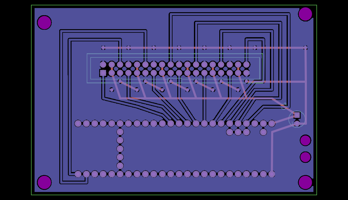
I thought I get some practice - expereance and have had a go at removing some vias… Hopefully the corcuit is correct 
And a general question; in an ideal situation, is it OK to have trace near the edge of or under an item that would be mounted on the board, e.g running a top trace under the edge of a mounted socket as I have done here?
Looks fine and yes its fine to run traces under compenents. Your timing is also good as I just finished testing the new teeny part which should be correct now. As well I changed the pins on your 36 pin header part to be .038 holes in pcb as well. From the image above however you still have the teensy mounted from the bottom. To fix that select the teeny (or better yet replace it with this one ), then in Inspector (lower right of the screen) check that the box pcb layer says top (not bottom as it likely says now). The vertical row of 5 pins should be on the right not the left in pcb view. Unfortunatly the orientation change of the teeny makes the routing much harder unless you can change the order of the pins on the connector.
Teensy 3.6 (Basic)_fixed.fzpz (42.7 KB)
Generic shrouded header - 36 pins.fzpz (11.0 KB)
this fixed version has a new part id so it should load along side your current one. The connector is the same part number so you will need to delete the current one. You will find among other changes that there are 5 new pins that were missing in the original but are on the board (they were present but not properly connected in the original part).
Peter
HI
I have had another go with the new part, the Teensy pins d31 and d32 are now on the opposite side, is the layout correct?
I have tried to copy the original layout and added some holes (this isn’t a big board) the corner holes are 4.2mm and the smaller (cable tie) holes are 2.2mm.
Although the holes I have added look like they are suitably spaced from the edge, in reality they are only have about a 2mm clearance, it doesn’t seem like a lot. How do designers decide where to put the (corner) mounting holes, i.e. how much edge clearance do they need?
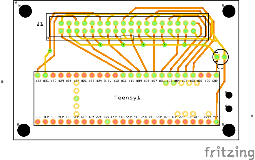
It still looks to be on the bottom to me. On my system with the Inspector pcb layer box set to top (which is what it should be) the part looks like this:
which indicates to me that you still have the part set to bottom. Since I don’t have a teensy I can’t verify this is correct. The thing to do is take a real part and position it as it would mount on the top of the board and see which orientation is correct. On mine if I hover over the right hand top pin it shows as D31:A14 Can1 … The right bottom pin is D32 SCK1 … Left top is Vin and left bottom is gnd. Which is the reverse of your current layout (and makes the routing unfortunatly much harder).
I’ll let one of our folks who make boards comment on this one because I don’t know.
Peter
That is the same way as they have it except you are rotated 180 degrees. You can tell theirs was correct because you an read the silkscreen and the color of the silkscreen is black but if it was on the bottom it would be gray.
@barnys1 The holes can be very close to the edge. The board shop will have a limit but it will likely be lower than your 2mm.
Ah! I never thought of rotating it 180 degrees to make the routing easier! So it looks like all is well then. Excellent.
Peter
The forum hasn’t let me post for the last couple of days for some reason, but I’ve fixed up the file, made a different one too and am expecting them from osh Park in a week or two. FWIW aisler has shut down for Christmas until the 8th and couldn’t help me. Thanks again for the tips everyone.