Where to find this "Stereo Audio Amplifier board" design!

Fritzing%20Audio%20Amplifier%20Board

“Stereo Audio Amplifier Board”
I want to download this module as .fzz but I never found it.
Anyone have any idea where I can add this board to Fritzing file!
what is the specific name for it?

A google search for “fritzing part Stereo Audio Amplifier Board” (under the images tab) says this is a PAM8403 6W STEREO AMPLIFIER. A google search for that indicates a part is available on github:

fritzing part PAM8403 6W STEREO AMPLIFIER

first hit:

I have no idea if the part is any good or not, but you should start there. If it doesn’t work, post again and I (or someone else) will have a look at the part.

Peter

1 Like

Probably not too interested in this part, I made it as Mono output. Of course, simple enough to change and use the second channel… It works as a baseline audio amp for my other projects needing Mono…

AMP_audio_LM386_RevA.fzz (14.4 KB)

1 Like

I needed this part too, so I went ahead and made it. Here’s the result!

PAM8403 6W Stereo Amplifier.fzpz (15.4 KB)

1 Like

Welcome aboard! Over all a usable part, it works as it stands. There are a few things that can be improved though. None of your svgs have layerIds. The only thing I know that affects is svg export, if someone exports a sketch as an svg (or one of the other formats) your part won’t be included because of the lack of layerIds. Schematic is missing terminalIds. That causes the wires to connect to the center of the pin rather than the end as is desirable:

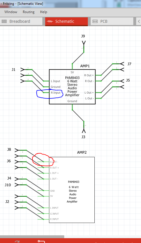
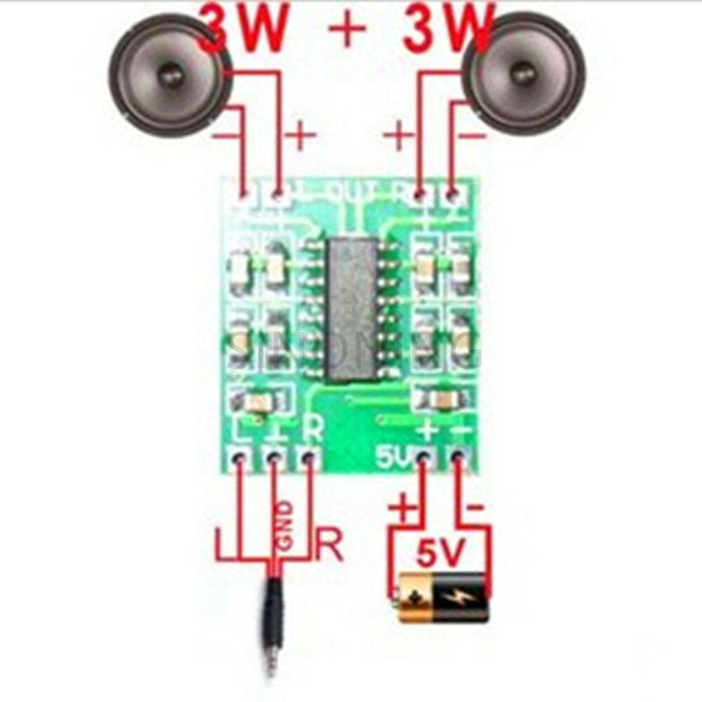
Your wires (circled in red) connect to the middle of the pin. Mine (circled in blue) connect to the terminalId on the end of the pin. As well I think your pcb svg is misaligned. While I don’t have one of these boards to look at, that is often the case, so I sucked down a poor quality jpeg of the board from ebay:

whose only redeeming feature is it is flat (the rest are tilted.) Importing it in to Inkscape and scaling it lets me place the pins (which I know are on exactly .1in centers over the pins in the jpeg to guess at where the pins should go. As I expected they appear to align on .1in boundaries which your pcb does not:

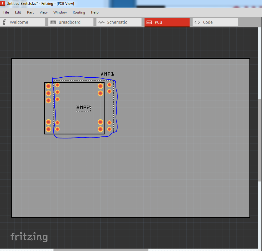
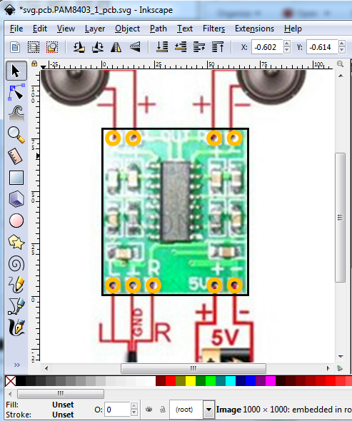
here amp2 (circled in blue) is your pcb svg. amp1 is what I think is the correct pcb aligned on .1 boundaries. You need to print out my part’s pcb at 1:1 scale and compare the output to a real board to see if my footprint is in fact correct. This is the jpeg image imported in to the pcb svg in Inkscape and scaled til it matches the three bottom connectors which I know to be 0.3in long over layed with the pads. The pads are set at multiples of 0.1in and appear to align with the jpg. I also increased the hole size of the pads (which is why mine are larger) to be 0.038in to take a standard .1in header pin (your original holes are 0.028444in which is too small for anything but small gauge wire.)

schematic had a bunch of unused connectors in it (probably left over from whatever it was cloned from) so I created an entirely new schematic from a template svg file. Convention is inputs on the left and outputs in the right, so I did it that way with .1 in long pins (as space in schematic is valuable) and the power pins on the top and bottom. I changed the moduleId and the file names to make mine a new part so you can load your original and mine beside each other (as I have done here) to compare the two. Here is the test sketch that created the images above:

PAM8403-test-Sketch.fzz (33.3 KB)

and the new part (which is in the temp parts bin of the above sketch as well):

PAM8403 6W Stereo Amplifier-improved.fzpz (9.0 KB)

Hope this helps and you make more parts :slight_smile: .

Peter

1 Like

This is good stuff – but beware! The grid holes are NOT ALIGNED to a standard grid on this part, which is VERY frustrating!

Do you know how to rename the groups in inkscape? I found many tutorials but was unable to figure it out without using a text editor – this seems to be the worst part!

I will take a look at the schematic, but the connections should have been the same as what I cloned it from… weird.

Yes that is frustrating! Time for the calipers to measure the real positions of the holes and update pcb to be accurate. It is even more frustrating to cut a PCB from a part then find the holes are in the wrong place, or the wrong size or no holes at all because the part is wrong, which has happened to folks more than once. I tend to leave breadboard on .1 centers so the wires are straight but accurate may be better in this case so it won’t connect to the breadboard as it won’t in real life!

With the warning that I am an Inkscape hack (I don’t know all the fancy graphic designer ways to make svgs because I only do Fritzing parts) I use xml editor in Inkscape and change the id field which renames the group. It is much the same as using a text editor to do it (and there probably is some graphical way I don’t know to do it as well) but it works. I tend to ungroup the whole svg as my first step and then regroup and rename the layerIds when I’m done. You will also see references to layers (sometimes even in the Fritzing doc such as it is) as far as I know in Fritzing layers mean a group id field, I think it may have a different meaning to competent Inkscape people :slight_smile:

Peter

@nebarnix I just started using Fritzing and I needed this part for my first project. Thanks so much for the original part. It looks great.

@vanepp I haven’t even finished the circuit yet so I don’t know how the issues would have affected the process, but thank you as well for the improvements. I made sure to download the updated file. Great to know this software has a community that helps one another improve things like this.