AlCon:
Does anyone know how can I get VL53L0X in .fz file? It’s a Time-of-flight Lidar sensor.
Thank you,
W.
AlCon:
Does anyone know how can I get VL53L0X in .fz file? It’s a Time-of-flight Lidar sensor.
Thank you,
W.
Welcome aboard! A google search for “fritzing part VL53L0X” turns up a version in the Adafruit fritzing library here:
there is another (which may be the adafuit one) in a Fritzing project here:
http://fritzing.org/projects/vl53l0x-ethernet-connections/fab/
In this case you would need to load the sketch in to Fritzing (the .fzz file) and in the temp parts bin you should find the part for the VL53L0X which you can use and/or export to save.
Peter
Thank you much.
Cheer,
W
If the existing parts don’t match your board, if you post a pointer to the mechanical data for the board you have modifying one of the existing parts shouldn’t be too difficult (at least for me.)
Peter
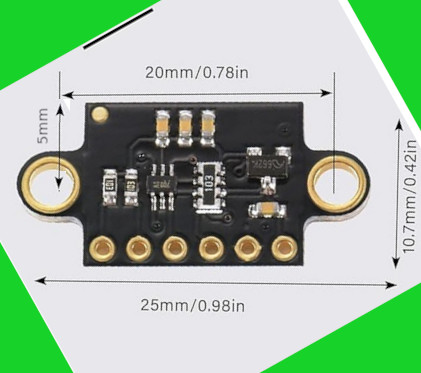
I’m wondering if this is enough info to make a version of the Adafruit part. The pin arrangement is the same. This board is more convenient for breadboard, especially if you have 2 of them on the board at the same time. It’s also easy to mount this vertical or horizontal.
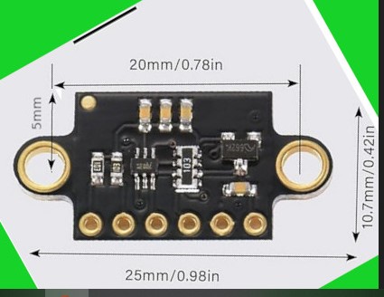
Buttom with measurements

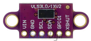
Top

The diameter of the holes is 3mm.
For reference, I’ve also used VL53L0X ToF laser distance sensor - small breakout which works well on pcbs, but only laying down.
I started on it though it’s still rough. I think it’s moving in the right direction. I used the adafruit as a basis and edited down, used the Checkparts script and edited further.
VL530X Time of Flight Distance Sensor.fzpz (7.0 KB)
A number of problems. Breadboard looks OK,
schematic has issues
the label field in the fzp file needs to change to A for assembly (which is what this is) the 4 side pins need terminalIds so the wire connects to the end of the pin not the middle as now. FritzingCheckPart.py should have flagged this (possibly only as a warning though.) Pcb also has issues
I would guess you don’t have a copper1 group in the svg as you can only connect on the bottom layer to the pins (the field that lets you change to the top layer is greyed out.)
Peter
Thanks! I tried reworking yesterday to correct the shapes but inkscape is too painful. Makes me consider getting a mac running and installing adobe illustrator. That’s bitter. The terminals in the svg were all over the place. All of them were there but duplicated and could not be altered. I tried making new ones, but got no further since other layers (breadboard, trying to fix the outline) were also a nightmare. This is as close as I got. I believe the pcb view and breadboard view work correctly.
VL530X Time of Flight Distance Sensor.fzpz (7.7 KB)
ANND, I think the breadboard is broken on this version.
I think Illustrator is worse. AFAIK you can’t (at least I haven’t found a way in their documentation) set things like scale and dimensions (their attitude appears to be “we will do that for you don’t worry about it” but Fritizng doesn’t like their choices.) Inkscape can be a pain but at least you can change anything you want.
Nothing immediately leaps out at me about breadboard. You are missing the layerId (which will cause the part to not export as an image) but I don’t see anything else alarming.
assuming this is the adafruit part as it says there is a Fritzing part in their repo here
that said I don’t see any board that matches yours when I do a google search for “vl530lox” and look at the images. There are a variety of options but none look to close to yours. Do you have a web site for the part you are trying to make?
Peter
Heh. My Illustrator days, and installation media are from the 1990s ![]() I doubt it supports svg. But sometimes, I’d rather hand edit postscript. I think the 1.1 version of inkscape I have has a few bugs.
I doubt it supports svg. But sometimes, I’d rather hand edit postscript. I think the 1.1 version of inkscape I have has a few bugs.
The board I’m trying to make is actually the purple / black one in the pictures above. I just hadn’t drawn the shape yet. I had to recover my parts database and only got this far. This version has an approximate if crappy correct shape for the for all views.
vl53l0x.fzpz (9.7 KB)
If you did fix it, if I try to take it apart in inkscape to compare all the attributes, will that work? I found structure seemed to be changed. For instance, I had never removed the ‘Breadboard’ label in that svg, but it ‘went away’ nevertheless.
Current version is 1.4 which is a lot better bug wise. An upgrade may be in order.
Ah! I had missed that original drawing. That makes more sense as it is one of the parts available in a google search. OK I downloaded your fzpz, and immediately see an issue in breadboard. The breadboard layerId is in the wrong place, it is an inkscape label which Fritzing ignores
it needs to be the group id (circled in green below it) in order to be recognized by Fritzing. You also want to do file->save as and choose plain svg rather than Inkscape svg to eliminate all the Inkscape specific stuff that can confuse Fritzing. In a while I will grab a copy of the original of this part and detail how I create one for you.
Peter
Ah! Thanks. This goes a long way to explain some of the odd behaviour.
Edit. It’s very odd that the label appears where it does in the xml when I edited the node number label and replaced it with ‘breadboard’. I suppose the editing applies to internal labels but the id persists. That is strange behaviour but I guess I’m just expecting it to behave as if it were editing the node itself.
Checking in xml editor is the best way to avoid that. The Inkscape labels show up there but so does the actual xml that it is emitting making errors like this obvious. I’m so used to the format of svgs that is more or less automatic for me.
Peter
OK here is a part and how I made it. Starting with my standard template breadboard file, first I set the size of the part to 25mmx10.7mm from your dimensions above.

then imported your jpeg file of the board in to Inkscape
locked height and width and reduced its size til it matches the outline as close as a in pitch will get.
then switch to mm and reduce it til the lengths are exactly the same.
it is slightly too short in height (not uncommon with jpegs so pull down slightly to match the height. Then set the color of the rectangle to match match the jpeg
we don’t need any SMD components so delete that.
then click on the rectangle an use Path->object to path to change it to a path, then set the appropriate number of nodes to make the path.
then move the nodes to the correct places
then move the image to the back so just the path is present.
The curves are straight lines at the moment so use the path tool to curve them.
That forms the basis of the board. Now Edit->select all, resize page to selection, Object->group and name the group id breadboard to complete breadboard.
Now for schematic. I use Randy’s Inkscape extension to make schematic (and while it works for me on Inkscape 1.4 on Windows it doesn’t for Randy and a fix is in the pipeline. We don’t know why it works for me.)
set the sizes first (note I set height too high here and reduced it later!) Add the name of the part to the label field.
then change tabs and set the pins for each side. Only 6 on the bottom in this case.
Then click apply and set the pin names.
click finish and it creates the svg (note you can’t have any other svg open while doing this, Inkscape sometimes gets confused and writes schematic to the wrong svg!) As noted I reduced the height of this to be more reasonable.
Do a save as->plain svg and schematic is done. Now copy the breadboard svg in to the pcb svg and edit it in Inkscape.
ungroup it and delete all the text and the sensor.
click on upper to select it, then in xml editor change the fill to none, stroke to #000000 and stroke-width to 10.
which creates the correct board outline on silkscreen.
Now change the two mounting holes to be only on silkscreen (they won’t be drilled, because if you don’t want mounting holes and they are drilled you need to modify the part. If they are only on silkscreen and you want them in your sketch you can drag in a hole from core parts–>pcb, place it over the circle in silkscreen and set the hole size correctly to drill the hole without having to modify the part.)
change this to this so the holes are only on silkscreen. Then remove the fill #ffffff from each of the connectors (that is ok in breadboard but not in pcb I don’t think!)

so we need to do a Edit->Select all then Edit->resize page to selection to resize the viewbox. Then group upper and the two circles in the silkscreen group.
and all the connectors in a copper1/copper0 group
and pcb is done. We can now File->save as->plain svg and pcb is done. Then create the necessary fzp file (I do it with a template and scripts that will define the connectors and edit from there.) That after being run through FritzingCheckPart.py to both check the part and remove the Inkscape additions (px in font names some others) that Fritzing objects to which results in this working part which should do what you want.
vl53lox.fzpz (4.9 KB)
unzipping the .fzpz will give you the .fzp file and all the svgs as usual. Hope this helps!
Peter
Thank you for this write up! I think I now know enough to not shoot myself in the foot ![]()
I’ll try the extension from Randy you mentioned and report back.
EDIT: one question. Why is copper0 within copper1 layer ? Is that just how the ‘group’ function works?
No, that is how Fritzing decides this is a THT board and copies one instance of the connector to both the top and bottom of the board. An SMD board only has copper1 (to put the copper on the top of the board.) As well separate copper0 and copper1 layers are supported (mostly for backwards compatibility I think) but you have to duplicate the pads on the other layer to make that work.
Peter
Thanks! Now that makes sense.