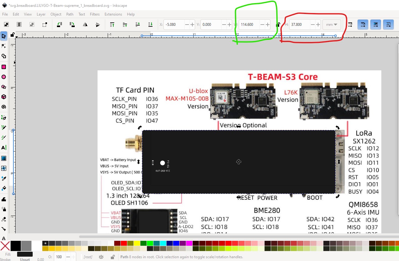
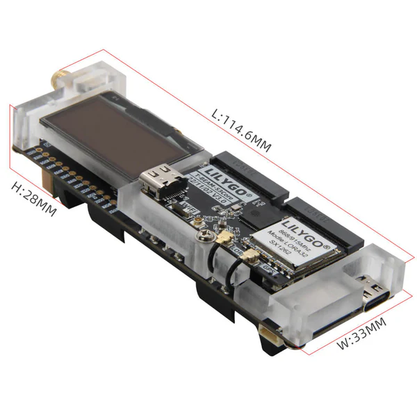
A couple of problems here. The dimensions don’t match the jpeg image. The docs claim the device is
114.6mmx33mm but that doesn’t match the jpeg image of the board. The dimensions that match the image are too large (37.8mm against 33mm)
It is possible to change the jpeg to match the stated dimensions but it is unclear that is correct.
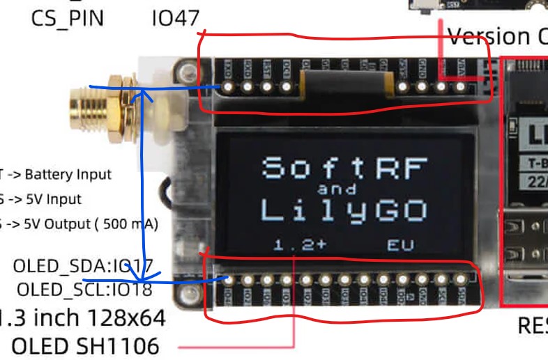
The second problem is that the labels on the board are unreadable (circled in red here.) If you have a board and can supply the text for the labels that would help. As well the spacing of between the pads (which should be on a 0.1in boundary I expect) would help in establishing the correct size.
Looks like I undersized the scaling a bit when I did the last image, increasing the scale to match the actual board size (which is obscured by the white plastic pads on the end) does drag the width down to the correct size. I will proceed to make a part.
This part should do what you want. As noted pcb view has been suppressed as not useful. The measurements are correct, they just extend to the end of the final SMA connector (not the board!) which I missed.