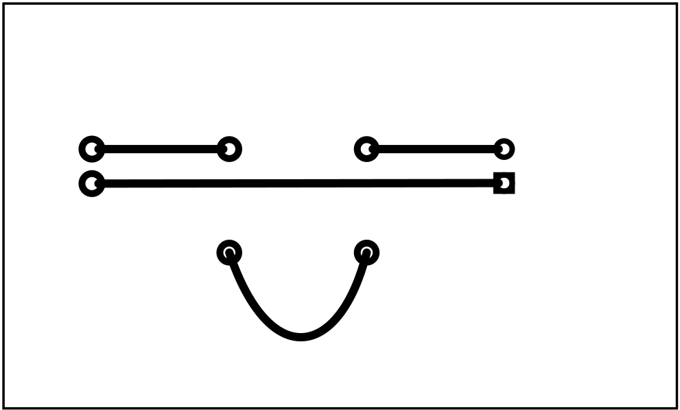
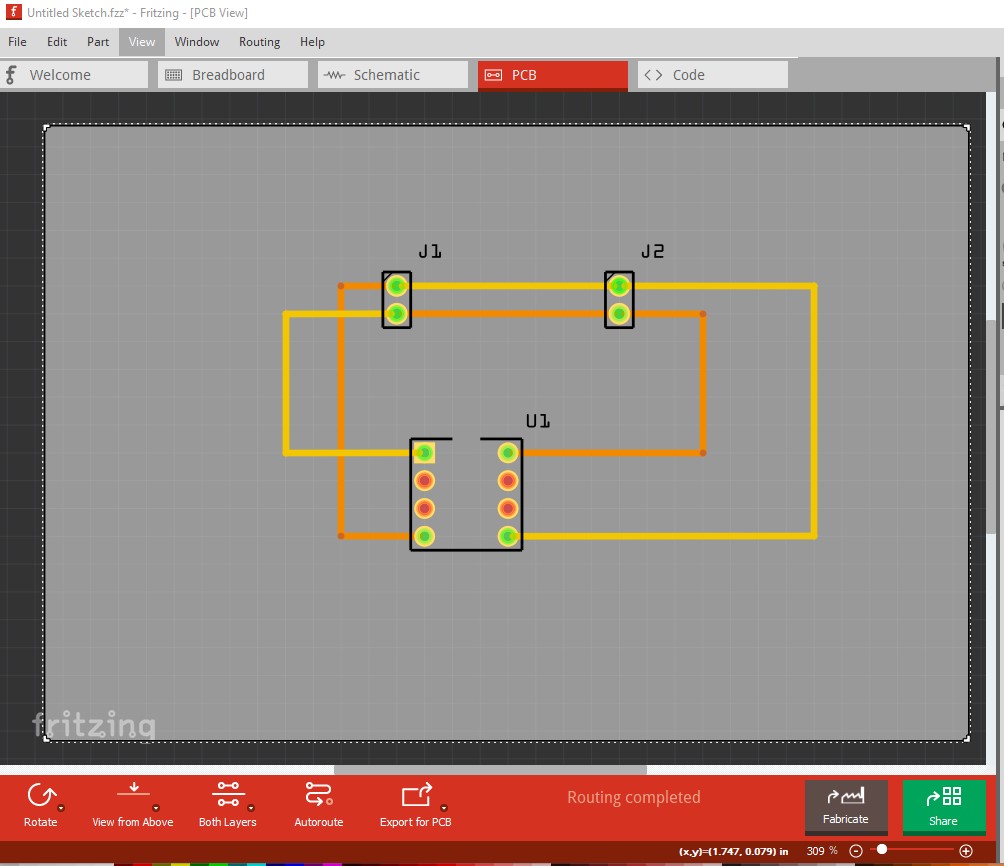
When I exported the PCB as an svg the traces appear to go through the pad and over the holes, this also appears in the PCB of the editor.
1 Like
Yes, although that is not particularly a problem as the hole will eliminate the overlap. What is a problem is that pcb looks to be using white for silkscreen when it should be black.
Fritzing pcb image
exported as a svg and displayed in Inkscape
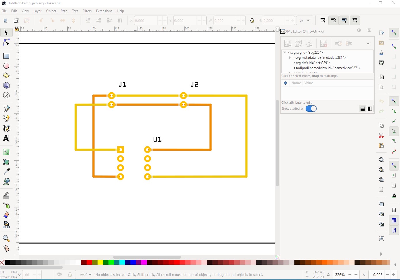
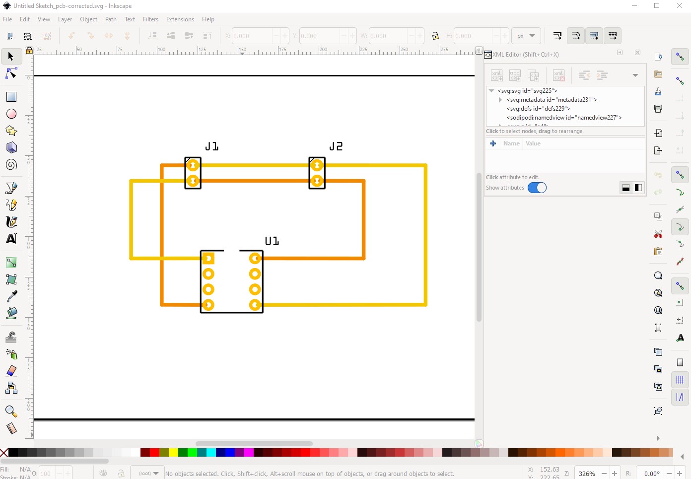
note the breaks in the traces in to the two headers and the IC and the lack of silkscreen. That is because the silkscreen has been set to white, when it is set to black as it should be the export is correct:
I’ll report this as a bug.
Peter