Hi, been at this for days. Can’t get it to work. Is this a bug? But in your response to the Jan 14 question, you answered one of my questions, “Click on one pin, and if both are connected they should turn yellow”. I expected this but it didn’t happen.
A: ground fill seed dialog box says it “collects” (not connects) all labeled “grd, ground” and “seeds”, the Vcc negative terminal is labelled “ground” and the blue encirclement is “hashed” opened appearing to connect to the gold “background” and so do the seeded connectors. This suggests all are connected. But, click on one they all don’t turn yellow, why?
B: if all seeds are connected to ground why don’t they turn “green” after a ground fill as in a trace connection?
I’m not really a high end user, nor have much elec experience, but I have a sketch done by someone else with ground fill, and if I click on one GND pin, all GND pins turn yellow.
In this sketch they stay red after the ground fill is applied.
If you want to post the .fzz here - 7th button - I can look at it.
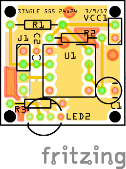
555 TIMER PCB.fzz (13.6 KB)
Thanks for the quick reply attached is the circuit. It would save a lot of traces and time if I could get ground fill to work.
Your help is appreciated,
Les
looks like the ground-fill is working alright to me… It looks like this circuit is not done, you have an RGB LED with only the green anode hooked up. But I’m sure you knew that.
Hi thanks for the quick reply. Opened the file you sent back, clicked the GF seed C1 pin1 expected to see GF seed pin1 of R2 turn yellow but didn’t. Apparently it did for you.
I read you don’t need traces for GF seeds. But if I set traces only on the bottom layer to all seeds and then ground fill, it seems to work, get islands, all GF seeds light when one is clicked, etc. and all orange traces disappear on top, top-bottom and faintly appear on bottom view.
Still wonder why ground fill seeds after ground fill do not turn “green” to show they are connected.
Though ground fill and seeds seem straight forward and simple (clearly not for me) I looked for tutorials to no avail and examples of circuits that I did find were not helpful
Hi all PLEASE HELP! been a this for weeks, Even bought
Simon Monk’s book and then bought the e-version cause I couldn’t wait to get the book hoping it would fully explain “ground fill” ( GF) and ground fill seeds" (GFS) a few sentences on GF, nothing on GFS, NO HELP! logically, and that may be my problem, if connectors are set as GFS then you ground fill, all are connected to a ground fill island, R3 pin 1, C1 -pin and U1 pin 1 “ground” are connected to the same island. I get that pin 0 of C2 is connected to an island that’s not connected to anything, so no connection to R1 or C1. What I dont get is why when I click R1, C1 and U1 dont light since they are on the same island? I must be missing something very simple.
You assign the ground seed to the pin on the part if you want it connected to the ground fill - right-click on pin -.
The ground pins only light when there is no ground fill, so you test it throughly before and then ground fill, but even after ground fill there should be a ratsnest dotted line still connecting grounds.
Pin ends only change from red to green when there is a physical connection.
You can link islands with links, or organise it so they can connect, or use one side of a double-sided board, or use a physical trace - red blob to red blob on the islands -, or you can set the ground fill keepout smaller so that it might be able to snake a connection, or use a via to the other side ground fill and then another via back to the other island.
You can upload it here - 7th button - and someone can look at it.
thanks, that was fast, I never get a ratsnest dotted line as you can see from the uploaded image. If I did then I would know they are connected and can remove them. I bet if I did remove them the connectors wouldn’t light. Don’t understand, “the ground pins only light when there is no ground fill…”.Thought you didn’t have to use a trace for seeds. Still don’t understand why if 3 connectors are touching the ground fill “yellow” they don’t light when you click one of them. I bought Simon Monk’s book hoping he would explain all of this but has very little on GFs and nothing on seeds. I get the part of linking the islands, that makes sense. How can I trust that the ground fill seeds are connected by the ground fill if they don’t light when one is clicked? Am i just supposed to accept that they are connected and submit my PCB for production?
Cant find anything online that fully explains how to use seeds and ground fill.Do you know of any site? Am I the only one with this problem and these questions or just dense?
hi thanks, downloaded the schematic v0.35, impressive especially the schematic which I suspect he did first. There is one interesting area, part labelled Q4, pin “source 3 basic FET…” looks like a ground fill seed but right click and the ground fill seed choice is not checked and there is no ratsnest line connecting this pin but it lights when the others are clicked?
there must be or should be a site that fully explains seeds and fills. The closest I have found is in Eagle and they mainly discuss ground fill planes.
btw its after I ground filled the sketch! before GND fill its is connected and set as a seed. after, no ratsnest connection but does what I thought it should, light when other seeds are clicked. after ground fill, GND fill seed after right click is not checked!
Sometimes I open the file and right-click that part and the faded ground seed text is not clicked - most of the time -, and other times it is ticked - rare -.
I vaguely remember having a problem a while back where I was having trouble setting ground seeds reliability, but I gave up on it because I don’t use GND fill on my projects.
You can go Routing/Ground Fill/Choose Ground Fill seeds and click on GND, and it shows you all the GND seeds.
You can also click the text in the bottom red bar.
You can also check the gerbers and output pics that they are actually there by looking at the drawing.
EDIT
I got the GND seeds back. I added a resistor to the PCB view and set one pin to GND seeds, and all came back.
From memory I think it was fine with small numbers of components, but this one with lots of components and it was unreliable.
Hi O/G, I THINK I SOLVED IT! Was always looking at this logically then it occurred to me maybe it was illogical or partly logical.
LOGICAL:
SET GROUND (GND) SEEDS THEN GND FILL, ALL SEEDS ARE THEN CONNECTED TO YELLOW FILL & TO EACH OTHER, SUPPOSEDLY, LOGICAL BUT WRONG
THEREFORE ALL CONNECTORS WITH “SEEDS” SHOULD TURN GREEN, LOGICALLY, THEY DON’T!
WHEN YOU CLICK ONE ALL SHOULD LIGHT, LOGICALLY, THEY DONT!
YOU ARE FORCED TO TRUST THEY ARE CONNECTED, LOGICALLY, BUT THEY ARE NOT!
YOU HAVE TO FIRST KNOW IT IS POSSIBLE. i know ground fill and seeds work, have a PCB done by Fritzing with connectors that are “unconnected” on the board but are connected to GND in reality.The image sent has these connectors “GREEN” WITH NO TRACE TO ANYTHING ON THE BOARD,must be a ground fill and seeds somewhere!.
I looked at the schematic you sent me and this person knows what he is doing just by looking at the schematic. His PCB has ratsnest lines, why? Because they are “trace” connected in the schematic! If you remove the ratsnest lines in the PCB, the connection is terminated in both views! But if you GND fill his PCB you see the “SEEDS” and the ratsnest lines. DONT DELETE THE LINES. as someone suggested, just click on one and move it, bend it, it disappears and the CONNECTORS TURN GREEN!
ILLOGICAL OR PARTLY LOGICAL:
SET GND FILL SEEDS, GND FILL NOW OR LATER
IN THE SCHEMATIC VIEW (why, I don’t know) make a trace from all SEEDS to wherever, to other seeds, to neg battery terminal, to ground, doesn’t matter.
IN THE PCB VIEW THESE TRACES ARE NOW RATSNEST LINES! (traces made in PCB view are ratsnest lines in the schematic view and vice versa, why, don’t know)
NOW GROUND FILL IF YOU HADN’T BEFORE, CONNECTORS WITH SEEDS AND RATSNEST LINES ARE STILL RED!
MOVE, BEND BUT DON’T DELETE THE RATSNEST (RNL) LINE! WHEN YOU RELEASE THE LEFT MOUSE AFTER MOVING OR BENDING THE RATSNEST LINE, DISAPPEARS!
THE SEED CONNECTORS TURN GREEN, HALLELUJAH! WHY NOW? I DON’T KNOW, AND YOU HAVE TO DO IT FOR EACH RNL
ALL CONNECTED SEEDS TO GND FILL WILL NOW LIGHT WHEN ONE IS “CLICKED” HALLELUJAH, AGAIN, I’M CURED!
IF YOU MAKE A MISTAKE YOU CANT JUST DESELECT “GROUND FILL SEEDS” OR REMOVE IT FROM A CONNECTOR, ONCE CONNECTED IT STAYS CONNECTED TO THE FILL! ONLY WAY I FOUND SO FAR IS TO DELETE ALL SEEDS AND START OVER!
While I don’t know anything about ground fills, this one I do know. This is true of all three views (and often a source of problems): a connection made in one view (breadboard, schematic or pcb) will be reflected as a rats nest line in to the other two views so you can make the same connection there. The gotchas appear to be around errors or possibly doing it in more than one view (I lean towards errors but am not sure). It is best practice to make all your connections in a single view and then save a copy of the board in that state because sometimes making a connection change in another view corrupts the Fritzing database and the only known cure is to start again (preferably from your saved only one view version although even that can be a pain.) I suspect (but don’t know for certain) that the changes that happen when you touch rats nest lines are probably the database being prodded and deciding there is a ground plane there that it needs to process. Once that is done the rats nest is routed and thus disappears.
Thanks Peter and many thanks O/G for the info that made me persist.
made my first PCB with seeds and ground fill, a thing of beauty!
BTW, FYI the previous off-white boards from Fritzing were elegant! Aisler’s boards are the traditional green with raised trace wires, lot cheaper but not elegant!. Aisler says I can get the others if I order 420 or more!